Just some colored traces on a board pic with RF shield removed:
(Grey: GND Pink: 12V Violet: 5V I do not really remember the rest…)
Logic board:
(This is the backside of the logic board, left side is bottom side.)Logic board, front side. This is actually a different H2’s board (with highly readable print on the chips), but should be the same.
In this article, we’ll create a short memory test for use on MSX/MSX2 machines to check the lower 32 KB of RAM. Why only the lower 32 KB of RAM? Because you can check the higher 32 KB using pure BASIC PEEKs and POKEs, and generally software won’t run if the higher 32 KB has defects. (Many games may still run even with defects in the lower 32 KB.)
It’s useful to have a test that can be run from BASIC and that can be typed into the machine in a couple minutes.
MSX bank switching
The MSX has a CPU that can only address 65536 addresses, but can have 64 KB of RAM and at least 16 KB of ROM. In a previous article, I mentioned that that is probably handled by copying ROM into RAM, but that is wrong. Instead, there is a chip that has a couple registers and enables/disables ROM/RAM chips based on the value of one of those registers.
On some MSX machines (but not the ones I tried) you may be able to read out that register from BASIC:
print inb(&ha8)
Summary: ROM/RAM can be switched in/out in 16 KB chunks, 0x0000-0x3fff, 0x4000-0x7fff, 0x8000-0xbfff, 0xc000-0xffff. There are four choices possible for each chunk. The register is 8 bits: 2 bits for the first chunk, 2 bits for the second chunk, etc.
There is another register (or rather another register for each slot) though, and it’s often used on MSX2 machines. This register is accessed in memory space, not I/O space. (Memory address 65535, requires that the correct slot be selected in the 0xc000-0xffff chunk.) This register gives us another four choices to select a different ROM/RAM for each choice already made. In other words, we have 4 pages (chunks), 4 slots (ROM/RAM choices), and for each slot, another 4 “subslots” (ROM/RAM choices). If you didn’t 100% understand that, don’t worry, I don’t actually think it’s comprehensible the way I wrote it. But you may still be able to follow the discussion below.
When we start BASIC on a 64 KB machine, we’ll probably have the lower 32 KB mapped to some kind of ROM, and the upper 32 KB mapped to RAM. BASIC then lets us use about 28 KB of that RAM and reserves about 4 KB for its own purposes, or so I assume. (The firmware selects the right slots and subslots to make this work for the machine in question, and the required numbers are different depending on the machine’s configuration. Also remember that there are RAM extension cartridges. During the boot phase, the firmware actively probes the 16 KB chunks to see if something is RAM or not. BTW, if the RAM is sufficiently bad, it won’t detect it as RAM at all and you’ll never see the boot screen.)
BASIC runs from ROM. If we disable that ROM (the “slot” containing the ROM) and instead enable RAM (the “slot” containing the RAM) on that “page” (chunk), we’ll be pulling the carpet from under BASIC’s feet. So if we run a command like this in BASIC:
out &ha8,0
The system will freeze immediately. So instead, we’ll be writing our memory test in assembler and poke it into memory, and then execute it.
We’ll be using a total of 9 instructions in our memory test program. Even if you have never seen Z80 assembly code, the following is almost all you need to know: “di” disables interrupts, just in case. “ei” re-enables interrupts. “ret” returns from our code, i.e., we’ll go back to BASIC. “ld” loads some 8-bit value to destination, from source. Numbers in (parentheses) are like dereference in C. (Except for in/out, you always uses parentheses there.) “cp” is compare argument with register “a”. (Some instructions require the use of register “a”.) “jp” is jump. “jp z,…” is “jump if equal”. “z” meaning, “if zero flag is set”.
Let’s first take a look at a short program that switches slots, undos the switch, and returns. It looks like this:
org 0c000h

di ; disable interrupts
ld a,0ffh ; put "255" in register "a" (the correct value depends on your machine!)
out (0a8h),a ; enable IO write, and put "0xa8" on the address bus and contents of register "a" on the data bus
;subslot
ld hl,0ffffh ; put "65535" in register "hl"
ld (hl),0ffh ; write "255" into *hl, i.e. into address 65535 (the correct value to write depends on your machine!)
;/subslot


; now undo everything:

ld a,0f0h ; put "240" in register "a" (the correct value depends on your machine!)
out (0a8h),a ; enable IO write, and put "0xa8" on the address bus and contents of register "a" (i.e., 240) on the data bus
;subslot
ld hl,0ffffh ; put "65535" in register "hl"
ld (hl),0f0h ; write "0" into *hl, i.e. into address 65535 (the correct value to write depends on your machine!)
;/subslot
ei ; enable interrupts
ret ; return to caller (BASIC)
This code can be assembled using “z80asm”, which is available in Debian’s repositories at least. z80asm outputs a file called “a.bin”. We can convert that file to unsigned 8-bit integers for use on BASIC data lines using od -t u1 a.bin.
Anyway, now we just need to add some code between the two snippets above. We want code that writes to memory addresses and then compares what was written. Here’s the annotated assembly code to do that:
ld hl,00h ; put 0 in register "hl"
write: ; this is a label that we can use in "jp" (jump) instructions
ld (hl),0ffh ; put 255 in *hl, i.e. address 0
inc hl ; increment hl register
ld a,h ; put high byte of "hl" register into "a" register
cp 080h ; check if the "a" register contains 0x80
jp z,done_writing ; if yes, that means we have incremented the hl register a bunch of times and it's time to go check if what we wrote earlier is still there (i.e. we've written 255 into 0x0000 to 0x7fff)
jp write ; if we reach this instruction, that means that the previous instruction didn't perform its conditional jump. this instruction jumps back to the instruction at the "write" label (ld (hl),0ffh). i.e., we haven't reached 0x8000 yet.

done_writing: ; this is a label
ld hl,00h ; put 0 in register "hl"
compare: ; this is a label
ld a,0ffh ; put 255 in register "a"
cp (hl) ; compare contents of register "a" with contents of *hl, i.e. memory address 0
jp nz,bad ; we put 255 in there earlier but this address contains something else now, that means we have bad memory
inc hl ; if we reach this instruction, that means that the previous instruction didn't perform its conditional jump. increment hl register
ld a,h ; put high byte of "hl" register into "a" register
cp 0c0h ; check if the "a" register contains 0xc0
jp z,done ; if yes, that means we have incremented the hl register a bunch of times and it's time to go home
jp compare ; if we reach this instruction, that means that the previous instruction didn't perform its conditional jump. this instruction jumps back to the instruction at the "compare" label (ld a,0ffh)

bad:
...

done:
...
Finding the correct values for I/O port A8 and memory port 65535
To make the assembled code work on your MSX, you will most likely have to change the values to be written into the A8 I/O register and the values to be written into address 65535 to select the correct sub-slot.
We want to access RAM, and it’s at slot 3, subslot 3. In BASIC, I get the following output:
?peek(65535)
15
This output is inverted. 15 is 0b00001111 in binary, but we should read this as 0b11110000. The lowest two bits specify the subslot for the 0x0000-0x3fff block. The subslot is set to 0b00, i.e. 0 here. Same for 0x4000-0x7fff. On page 0x8000-0xbfff, we see that subslot 0b11, i.e., 3 is selected. Same for 0xc000-0xffff. This is as expected — the above table from the MSX wiki page specifies that all RAM is at subslot 3 (of slot 3).
If we want the lower pages to point to RAM, we not only have to set the A8 register to 3 (because all the RAM is at slot 3), we also have to select subslot 3.
I.e., to set the subslots for all four 16 KB chunks (“pages”) to use RAM, which is at slot 3 subslot 3, we have to write 0b11111111. To revert this, we have to write 0b11110000 (our peek showed 15 (0b00001111) at memory address 65535, but this is inverted, hence 0b11110000).
Customizing the memory test
In the above code, we write 0xff to all addresses, and then later check if 0xff is still there. However, one very common type of memory fault is “stuck bits”, where memory bits are always stuck at 1, even if we’d written 0. In order to test that, I recommend that you change “ld (hl),0ffh” and “ld a,0ffh” under the “write” and “compare” labels to different values.
We also have to think about what to do if we have encountered bad memory. One easy thing we can do is generate an audible click. (May be somewhat faint.) Here’s the code to do that:
bad:
ld a,15
out (0abh),a
ld a,14
out (0abh),a
ld a,15
Writing 15 and then 14 to 0xAB produces a click. You can do this in BASIC too:
out &hab,15:out &hab,14
Alternatively, we could write the memory address that contained something unexpected into some memory location, for example like this:
ld de,0c100h ; memory address to write to
ld a,h
ld (de),a
inc de
ld a,l
ld (de),a
This would write the significant byte of the failed address to 0xc100 and the insignificant byte to 0xc101.
Putting it all together
Here’s the assembly code for the whole test:
org 0c000h

di
ld a,0ffh
out (0a8h),a
;subslot
ld hl,0ffffh
ld (hl),0ffh
;/subslot
ld hl,00h
write:
ld (hl),0
; ld (hl),l ; alternative code, fills RAM with 0x00-0xff, 0x00-0xff, ...
; nop
inc hl
ld a,h
cp 080h
jp z,done_writing
jp write

done_writing:
ld hl,00h
compare:
ld a,0
; ld a,l ; alternative code, see above
; nop
cp (hl)
jp nz,bad
inc hl
ld a,h
cp 080h
jp z,done
jp compare

bad: ; audible click version
ld a,15
out (0abh),a
ld a,14
out (0abh),a
ld a,15

done:
ld a,0f0h
out (0a8h),a
;subslot
ld hl,0ffffh
ld (hl),0f0h
;/subslot
ei
ret
And here’s the short BASIC loader:
10 i=49152
20 read j
30 if j=-1 then goto 80
40 poke i,j
50 i=i+1
60 goto 20
70 data 243,62,255,211,168,33,255,255,54,255,33,0,0,54,255,35,124,254,128,202,25,192,195,13,192,33,0,0,62,255,190,194,44,192,35,124,254,128,202,54,192,195,28,192,62,16,211,171,62,14,211,171,62,15,62,240,211,168,33,255,255,54,240,251,201,-1
80 def usr1=49152

run
Ok.
x=usr1(0)
Ok.
If you get “Ok.” after “x=usr1(0)”, the machine hasn’t crashed (which means your slot and subslot selections were correct). If you heard a click, your memory is probably defective.
The click may be hard to hear, so maybe try running “x=usr1(0)” in a loop:
My Hitachi MB-H2 MSX machine has an analog RGB port that produces a 15.6 KHz CSYNC (combined horizontal and vertical) signal and analog voltages indicating how red, green or yellow things are.
I recently unearthed my old LCD from 2006 or so and decided to see if I could get it to sync if I just massaged the CSYNC signal a bit to bring it to TTL levels and connected a VGA cable.
(Technical details: when you connect a VGA cable to a monitor that is powered on, you will often first of all see a message like “Cable not connected”. To get past that problem, you first have to ground a certain pin on the VGA connector. I found that female Dupont connectors fit reasonably well on male VGA connectors so I just used a cable with female Dupont connectors on both ends to connect the two relevant pins. I’m not sure if it’s the same pin on all monitors. You can find the pin by looking for a pin that should be GND according to the VGA pinout but actually has some voltage on it. Don’t blame me if you break your Dupont connectors by following this advice.)
Unfortunately, that didn’t work. I got “Input not supported”, and I am reasonably sure that is because my monitor doesn’t support 15 KHz signals. Aw, why’d I even bother taking it out of storage?
So what do we do… Well there is this library (PicoVGA) that produces VGA signals using the Raspberry Pi Pico’s PIOs. Raspberry Pi Picos are extremely cheap, just about 600 yen per piece where I am.
Yes, this is animated and super smooth.
Damn, I’ve seen this in videos, but seeing this in real life, a tiny, puny microcontroller generating fricking VGA signals! Amazing. Just last year I was playing around with monochrome composite output on an Arduino Nano, and even that was super impressive to me! (Cue people reading this 20 years in the future and laughing at the silly dude with the retro microcontroller from year-of-the-pandemic 2020. I’m sure microcontrollers in the 2040s will have 32 cores and dozens of pins with built-in 1 GHz DACs and ADCs and mains voltage tolerance, and will be able to generate a couple streams of 4K video ;D)
Some boring technical notes I took before embarking on the project, feel free to skip this section
Is the Pico’s VGA library magic? Yes, definitely. Can we add our own magic to simultaneously capture video and output it via the VGA library? It sure looks like it! Why?
The Pico has two CPU cores, and the VGA library uses just one of them, the second core
Dual-core microcontroller, that’s craziness
We may be able to use the second core a little bit anyway (“If the second core is not very busy (e.g. when displaying 8-bit graphics that are simply transferred using DMA transfer), it can also be used for the main program work.”)
We will indeed be working with 8-bit graphics simply transferred using DMA
The Pico has two PIO controllers, and the VGA library uses just one (“The display of the image by the PicoVGA library is performed by the PIO processor controller. PIO0 is used. The other controller, PIO1, is unused and can be used for other purposes.”)
However:
We possibly won’t be able to use DMA all that much (“Care must also be taken when using DMA transfer. DMA is used to transfer data to the PIO. Although the transfer uses a FIFO cache, using a different DMA channel may cause the render DMA channel to be delayed and thus cause the video to drop out. A DMA overload can occur, for example, when a large block of data in RAM is transferred quickly. However, the biggest load is the DMA transfer of data from flash memory. In this case, the DMA channel waits for data to be read from flash via QSPI and thus blocks the DMA render channel.”)
If we use PIO and DMA for capturing video-in, we might run into trouble there
However, using DMA to capture and another DMA transfer to transfer the data to VGA out sounds somewhat inefficient; maybe it’s possible to directly transfer from capture PIO to VGA PIO? Would require modifications to the VGA library, which doesn’t sound so great right now (we didn’t do this)
That said, it’s likely that capturing without the use of PIO would be fast enough, generally speaking. The “pixel clock” for a 320×200 @ 60 Hz signal is between 4.944 and 6 MHz according to https://tomverbeure.github.io/video_timings_calculator (select 320×200 / 60 in the drop-down menu), depending on some kind of mode that I don’t know anything about. According to our oscilloscope capture of a single pixel on one of the color channels (DS1Z_QuickPrint22.png), we get about 5.102 MHz. Let’s take that value. We’ll hopefully be able to calculate the exact value at some point. (Yeah, the TMS59918A/TMS59928A/TMS59929A datasheet actually (almost) mentions the exact value! “The VDP is designed to operate with a 10.738635 (± 0.005) MHz crystal”, “This master clock is divided by two to generate the pixel clock (5.3 MHz)”. So it’s 5.3693175 MHz, thank you very much.)
This means that we have to be able to capture at exactly that frequency. From our previous experimental logic analyzer (which doesn’t use PIO) we were more than capable of capturing everything going on with our Z80 CPU — we had multiple samples of every single state the CPU happened to be in, and the CPU ran at 3.58 MHz. (However, if the VGA library chooses to set the CPU to use a lower clock frequency, we may run into problems. It’s possible to prevent the library from adjusting the clock frequency, but maybe that will impact image quality.) The main part of the code looked like this:
for (i = 0; i < LOGIC_BUFFER_LEN; i++) {
    logic_buffer[i] = gpio_get_all() & ALL_REGULAR_GPIO_PINS;
}
To capture video, we’d like to post-process our capture just a little bit, to convert it to 3-3-2 RGB. Or we could post-process our capture during VSYNC, but that would be a rather tight fit, with only 1.2 ms to work with. (Actually, our signal’s VSYNC pulse is even shorter than that, but there’s nothing on the RGB pins for a while before and after that.)
So our loop might look like this. (Note, the code I ended up writing looks reasonably similar to this, which is why I’m including this here.)
for (x = 0; x < 320; x++) {
    pixel = gpio_get_all();
    red = msb_table_inverted[((pixel & R_MASK) >> R_SHIFT) << R_SHIFT];
    green = msb_table_inverted[((pixel & G_MASK) >> G_SHIFT) << G_SHIFT];
    blue = msb_table_inverted[((pixel & B_MASK) >> B_SHIFT) << B_SHIFT];
    capture[y][x] = red | (green << 3) | (blue << 6);
}
Where msb_table_inverted is a lookup table to convert our raw GPIO input to the proper R/G/B values. This depends on how we do the analog to digital conversion, so the loop might look slightly different in the end.
Well, how likely is it that this will produce a perfectly synced capture? About 0% in my opinion. If we’re too fast, we’ll get a horizontally compressed image. If we’re too slow, the image will be wider than it should be, and more importantly, cut off on the right side. In the first case, we may be able to improve the situation by adding the right amount of NOPs. In the second case, we could reduce the amount of on-the-fly post-processing, and do stuff during HBLANK or VBLANK instead. In addition, we might miss a few pixels on the left side if we can’t begin capturing immediately when we get our HSYNC interrupt. How likely is this to succeed? It might work, I think.
The PIOs can also be used without DMA. (Instead of using DMA, we’d use functions like pio_sm_get_blocking().) With PIO, we can get perfect timing, which would be really great to have. We can’t off-load any arithmetic or bit twiddling operations, the PIOs don’t have that. So let’s dig in and run some experiments.
You can specify the number of samples you’d like to read (const uint CAPTURE_N_SAMPLES = 96)
You can specify the number of pins you’d like to sample from (const uint CAPTURE_PIN_COUNT = 2)
You can specify the frequency you’d like to read at (logic_analyser_init(pio, sm, CAPTURE_PIN_BASE, CAPTURE_PIN_COUNT, 1.f), where “1.f” is a divider of the system clock. I.e., this will capture at system clock speed. We can specify a float number here.)
The PIO input is (mostly?) independent from what else you have going on on that pin, so the code of course proceeds to configure a PWM signal on a pin, and to capture from that same pin. Bonkers!
Well, let’s cut to the chase, shall we? I took parts of the logic_analyser code to capture the input from RGB, then wrote some code to massage the captured data a little bit, and then output everything using PicoVGA at a higher resolution. After some troubleshooting, I got a readable signal!
However, my capture has wobbly scanlines. Which is why there might be a part 2. And since it’s wobbly, I spent even less effort on the analog to digital conversion than I’d originally planned, which was already rather “poor man” (more on that later, because the code assumes that circuit exists).
I’m triggering the capture by looking for a positive to negative transition. (That’s already two out of the three instructions my PIO program consists of, one to wait for positive, one to wait for negative.) I currently don’t really know why my scanlines are wobbly. I had a few looks with the oscilloscope to see if there’s anything wrong in my circuit that converts CSYNC to TTL levels — for example, slow response from the transistor. But I didn’t find anything so far. :3 It’s of course entirely possible that the source signal is wonky. I’ve never had a chance to connect my MSX to a monitor that supports 15 KHz signals. (Now that’s a major TODO right there.) Of course there are other ways to check if the signal is okay.
We could also (hopefully) get rid of the wobbling by only paying attention to the VSYNC and timing scanlines ourselves, for example by generating them using the Pico’s PWM. As seen in the original logic_analyser.c code! But that’s something for part 2 I guess.
BTW, it’s unlikely that the wobbliness is being caused by a problem with the code or resource contention. I tested this by switching the capture to an off-screen buffer after a few seconds. The screen displayed the last frame captured into the real framebuffer, and was entirely static. I.e., I added code like this into the main loop (which you will see below):
What I actually planned to do: the program I wrote expects four different levels of red, green, and blue. There are three pins per color, and if all pins of a color are 0, that means that color is 0, if only one is 1, that’s still quite dark, if two are 1, that’s somewhat bright, and if all three are 1, then that’s bright. The program then converts that into two bits (0, 1, 2, 3); PicoVGA works with 8-bit colors, 3 bits for red, 3 bits for green, 2 bits for blue. That means that we can capture all the blue we need, and for red and green we could scale the numbers a bit. However, I shelved that plan for now, because I don’t even have enough potentiometers at the moment, and if the signal is as wobbly as it is, that’s just putting lipstick on a pig. Instead, I just took a single color (blue, just because that was less likely to short my MacGyver wiring), and feed that into all colors’ “bright” pin.
As my MSX’s RGB signal voltages are a bit funky (-0.7 to 0.1 IIRC), I converted that to something the Pico can understand using a simple class A-kinda amplifier. The signal gets inverted by this circuit, but that’s fine for a POC. Completely blue will be black, and vice versa.
So here’s the code:
#include "include.h"

#include <stdio.h>
#include <stdlib.h>

#include "pico/stdlib.h"
#include "hardware/pio.h"
#include "hardware/dma.h"
#include "hardware/structs/bus_ctrl.h"

// Some logic to analyse:
#include "hardware/structs/pwm.h"

const uint CAPTURE_PIN_BASE = 9;
const uint CAPTURE_PIN_COUNT = 10; // CSYNC, 3*R, 3*G, 3*B

const float PIXEL_CLOCK = 5369.3175f; // datasheet (TMS9918A_TMS9928A_TMS9929A_Video_Display_Processors_Data_Manual_Nov82.pdf) page 3-8 / section 3.6.1 says 5.3693175 MHz (10.73865/2)
// from same page on datasheet
// HORIZONTAL                   PATTERN OR MULTICOLOR   TEXT
// HORIZONTAL ACTIVE DISPLAY    256                     240
// RIGHT BORDER                 15                      25
// RIGHT BLANKING               8                       8
// HORIZONTAL SYNC              26                      26
// LEFT BLANKING                2                       2
// COLOR BURST                  14                      14
// LEFT BLANKING                8                       8
// LEFT BORDER                  13                      19
// TOTAL                        342                     342

const uint INPUT_VIDEO_WIDTH = 308; // left blanking + color burst + left blanking + left border + active + right border

// VERTICAL                     LINE
// VERTICAL ACTIVE DISPLAY      192
// BOTTOM BORDER                24
// BOTTOM BLANKING              3
// VERTICAL SYNC                3
// TOP BLANKING                 13
// TOP BORDER                   27
// TOTAL                        262

const uint INPUT_VIDEO_HEIGHT = 240; // top blanking + top border + active + 1/3 of bottom border
const uint INPUT_VIDEO_HEIGHT_OFFSET_Y = 40; // ignore top 40 (top blanking + top border) scanlines
// we're capturing everything there is to see on the horizontal axis, but throwing out most of the border on the vertical axis
// NOTE: other machines probably have different blanking/border periods

const uint CAPTURE_N_SAMPLES = INPUT_VIDEO_WIDTH;

const uint OUTPUT_VIDEO_WIDTH = 320;
const uint OUTPUT_VIDEO_HEIGHT = 200;

static_assert(OUTPUT_VIDEO_WIDTH >= INPUT_VIDEO_WIDTH);
static_assert(OUTPUT_VIDEO_HEIGHT >= INPUT_VIDEO_HEIGHT-INPUT_VIDEO_HEIGHT_OFFSET_Y);

uint offset; // Lazy global variable; this holds the offset of our PIO program

// Framebuffer
ALIGNED u8 rgb_buf[OUTPUT_VIDEO_WIDTH*OUTPUT_VIDEO_HEIGHT];

static inline uint bits_packed_per_word(uint pin_count) {
    // If the number of pins to be sampled divides the shift register size, we
    // can use the full SR and FIFO width, and push when the input shift count
    // exactly reaches 32. If not, we have to push earlier, so we use the FIFO
    // a little less efficiently.
    const uint SHIFT_REG_WIDTH = 32;
    return SHIFT_REG_WIDTH - (SHIFT_REG_WIDTH % pin_count);
}

void logic_analyser_init(PIO pio, uint sm, uint pin_base, uint pin_count, float div) {
    // Load a program to capture n pins. This is just a single `in pins, n`
    // instruction with a wrap.
    uint16_t capture_prog_instr[3];
    capture_prog_instr[0] = pio_encode_wait_gpio(false, pin_base);
    capture_prog_instr[1] = pio_encode_wait_gpio(true, pin_base);
    capture_prog_instr[2] = pio_encode_in(pio_pins, pin_count);
    struct pio_program capture_prog = {
            .instructions = capture_prog_instr,
            .length = 3,
            .origin = -1
    };
    offset = pio_add_program(pio, &capture_prog);

    // Configure state machine to loop over this `in` instruction forever,
    // with autopush enabled.
    pio_sm_config c = pio_get_default_sm_config();
    sm_config_set_in_pins(&c, pin_base);
    sm_config_set_wrap(&c, offset+2, offset+2); // do not repeat pio_encode_wait_gpio instructions
    sm_config_set_clkdiv(&c, div);
    // Note that we may push at a < 32 bit threshold if pin_count does not
    // divide 32. We are using shift-to-right, so the sample data ends up
    // left-justified in the FIFO in this case, with some zeroes at the LSBs.
    sm_config_set_in_shift(&c, true, true, bits_packed_per_word(pin_count)); // push when we have reached 32 - (32 % pin_count) bits (27 if pin_count==9, 30 if pin_count==10)
    sm_config_set_fifo_join(&c, PIO_FIFO_JOIN_RX); // TX not used, so we can use everything for RX
    pio_sm_init(pio, sm, offset, &c);
}

void logic_analyser_arm(PIO pio, uint sm, uint dma_chan, uint32_t *capture_buf, size_t capture_size_words,
                        uint trigger_pin, bool trigger_level) {
    pio_sm_set_enabled(pio, sm, false);
    // Need to clear _input shift counter_, as well as FIFO, because there may be
    // partial ISR contents left over from a previous run. sm_restart does this.
    pio_sm_clear_fifos(pio, sm);
    pio_sm_restart(pio, sm);

    dma_channel_config c = dma_channel_get_default_config(dma_chan);
    channel_config_set_read_increment(&c, false);
    channel_config_set_write_increment(&c, true);
    channel_config_set_dreq(&c, pio_get_dreq(pio, sm, false)); // pio_get_dreq returns something the DMA controller can use to know when to transfer something

    dma_channel_configure(dma_chan, &c,
        capture_buf,        // Destination pointer
        &pio->rxf[sm],      // Source pointer
        capture_size_words, // Number of transfers
        true                // Start immediately
    );

    pio_sm_exec(pio, sm, pio_encode_jmp(offset)); // just restarting doesn't jump back to the initial_pc AFAICT
    pio_sm_set_enabled(pio, sm, true);
}

void blink(uint32_t ms=500)
{
    gpio_put(PICO_DEFAULT_LED_PIN, true);
    sleep_ms(ms);
    gpio_put(PICO_DEFAULT_LED_PIN, false);
    sleep_ms(ms);
}

// uint8_t msb_table_inverted[8] = { 3, 3, 3, 3, 2, 2, 1, 0 };
uint8_t msb_table_inverted[8] = { 0, 1, 2, 2, 3, 3, 3, 3 };

void post_process(uint8_t *rgb_bufy, uint32_t *capture_buf, uint buf_size_words)
{
    uint16_t i, j, k;
    uint32_t temp;
    for (i = 8, j = 0; i < buf_size_words; i++, j += 3) { // start copying at pixel 24 (8*3) (i.e., ignore left blank and color burst, exactly 24 pixels).
        temp = capture_buf[i] >> (2+1); // 2: we're only shifting in 30 bits out of 32, 1: ignore csync
        rgb_bufy[j] = msb_table_inverted[temp & 0b111]; // red
        rgb_bufy[j] |= (msb_table_inverted[(temp & 0b111000) >> 3] << 3); // green
        rgb_bufy[j] |= (msb_table_inverted[(temp & 0b111000000) >> 6] << 6); // blue
        temp >>= 10; // go to next sample, ignoring csync
        rgb_bufy[j+1] = msb_table_inverted[temp & 0b111]; // red
        rgb_bufy[j+1] |= (msb_table_inverted[(temp & 0b111000) >> 3] << 3); // green
        rgb_bufy[j+1] |= (msb_table_inverted[(temp & 0b111000000) >> 6] << 6); // blue
        temp >>= 10; // go to next sample, ignoring csync
        rgb_bufy[j+2] = msb_table_inverted[temp & 0b111]; // red
        rgb_bufy[j+2] |= (msb_table_inverted[(temp & 0b111000) >> 3] << 3); // green
        rgb_bufy[j+2] |= (msb_table_inverted[(temp & 0b111000000) >> 6] << 6); // blue
    }
}

int main()
{
    uint16_t i, y;

    gpio_init(PICO_DEFAULT_LED_PIN);
    gpio_init(CAPTURE_PIN_BASE);
    gpio_set_dir(PICO_DEFAULT_LED_PIN, GPIO_OUT);
    gpio_set_dir(CAPTURE_PIN_BASE, GPIO_IN);

    blink();

    // initialize videomode
    Video(DEV_VGA, RES_CGA, FORM_8BIT, rgb_buf);

    blink();

    // We're going to capture into a u32 buffer, for best DMA efficiency. Need
    // to be careful of rounding in case the number of pins being sampled
    // isn't a power of 2.
    uint total_sample_bits = CAPTURE_N_SAMPLES * CAPTURE_PIN_COUNT;
    total_sample_bits += bits_packed_per_word(CAPTURE_PIN_COUNT) - 1;
    uint buf_size_words = total_sample_bits / bits_packed_per_word(CAPTURE_PIN_COUNT);
    uint32_t *capture_buf0 = (uint32_t*)malloc(buf_size_words * sizeof(uint32_t));
    hard_assert(capture_buf0);
    uint32_t *capture_buf1 = (uint32_t*)malloc(buf_size_words * sizeof(uint32_t));
    hard_assert(capture_buf1);

    blink();

    // Grant high bus priority to the DMA, so it can shove the processors out
    // of the way. This should only be needed if you are pushing things up to
    // >16bits/clk here, i.e. if you need to saturate the bus completely.
    // (Didn't try this)
//     bus_ctrl_hw->priority = BUSCTRL_BUS_PRIORITY_DMA_W_BITS | BUSCTRL_BUS_PRIORITY_DMA_R_BITS;

    PIO pio = pio1;
    uint sm = 0;
    uint dma_chan = 8; // 0-7 may be used by VGA library (depending on resolution)

    logic_analyser_init(pio, sm, CAPTURE_PIN_BASE, CAPTURE_PIN_COUNT, (float)Vmode.freq/PIXEL_CLOCK);

    blink();

    // 1) DMA in 1st scan line, wait for completion
    // 2) DMA in 2nd scan line, post-process previous scan line, wait for completion
    // 3) DMA in 3rd scan line, post-process previous scan line, wait for completion
    // ...
    // n) Post-process last scanline

    // I'm reasonably sure we have enough processing power to post-process scanlines in real time, we should have about 80 us.
    // At 126 MHz each clock cycle is about 8 ns, so we have 10000 instructions to process about 320 bytes, or 31.25 instructions per byte.
    while (true) {
        // "Software-render" vsync detection... I.e., wait for low on csync, usleep for hsync_pulse_time+something, check if we're still low
        // If we are, that's a vsync pulse!
        // This works well enough AFAICT
        while (true) {
            while(gpio_get(CAPTURE_PIN_BASE)); // wait for negative pulse on csync
            sleep_us(10); // hsync negative pulse is about 4.92 us according to oscilloscope, so let's wait a little longer than 4.92 us
            if (!gpio_get(CAPTURE_PIN_BASE)) // we're still low! this must be a vsync pulse
                break;
        }
        for (y = 0; y <= INPUT_VIDEO_HEIGHT_OFFSET_Y; y ++) { // capture and throw away first 40 scanlines, capture without throwing away 41st scanline
            logic_analyser_arm(pio, sm, dma_chan, capture_buf0, buf_size_words, CAPTURE_PIN_BASE, true);
            dma_channel_wait_for_finish_blocking(dma_chan);
        }
        for (y = 1; y < (INPUT_VIDEO_HEIGHT-INPUT_VIDEO_HEIGHT_OFFSET_Y)-1; y += 2) {
            logic_analyser_arm(pio, sm, dma_chan, capture_buf1, buf_size_words, CAPTURE_PIN_BASE, true);
            post_process(rgb_buf + (y-1)*OUTPUT_VIDEO_WIDTH, capture_buf0, buf_size_words);
            dma_channel_wait_for_finish_blocking(dma_chan);

            logic_analyser_arm(pio, sm, dma_chan, capture_buf0, buf_size_words, CAPTURE_PIN_BASE, true);
            post_process(rgb_buf + y*OUTPUT_VIDEO_WIDTH, capture_buf1, buf_size_words);
            dma_channel_wait_for_finish_blocking(dma_chan);
        }
        post_process(rgb_buf + (y-2)*OUTPUT_VIDEO_WIDTH, capture_buf0, buf_size_words);
    }
}
Replace vga_hello/src/main.cpp with the above file and recompile (make program.uf2). Maybe this post will help if you are on something that isn’t Windows and can’t get this to compile.
Explanation
The PIO program is generated in the logic_analyser_init function. Here it is again:
First we wait for a “false” (low) signal. Then a “true” (high) signal. Then we read. Okay… but that doesn’t make any sense, does it? No, it doesn’t, but maybe with the following bit of code:
sm_config_set_wrap(&c, offset+2, offset+2); // do not repeat pio_encode_wait_gpio instructions
sm_config_set_wrap is used to tell the PIOs how to loop the PIO program. And in this case, we loop after we have executed the instruction at offset+2, and we jump to offset+2. The instruction at offset+2 is the “in” instruction. That is, we just keep executing the “in” instruction, except the first time. The first time, we wait for low on CSYNC, then wait for high on CSYNC, and then (as this state means that the CSYNC pulse is over) we keep reading as fast as we can (at the programmed PIO speed).
Results
Let’s take a look at the results. Remember, we’re converting to monochrome, and only looking at the blue channel. Remember that our super lazy “analog frontend” is super lazy, and the potentiometer has to be fine-tuned to get to a sweet spot that allows everything on the screen to be displayed.
The composite signal. Black looking very… let’s call it RGB, is one of the things that motivated me to check if I can get monitor output to work. The other thing is the jailbars. The jailbars are more prominent when showing a dark color.This is before tuning the capture parameters to ignore HBLANK and VBLANK, so we’re slightly cut off at the bottom and on the right. We’re only feeding into the pin for green here. Everything where blue is at zero intensity is green (top VBLANK and left HBLANK and black characters), and everything where blue is at full intensity, is black. I was running off a slightly wrong pixel clock here. You can see that the boundary between HBLANK green and black is fuzzy. On some scanlines we start a pixel (or fraction of a pixel) early, on others a pixel (or fraction thereof) late. On the next frame, this moves a little. It’s like there’s a somewhat low-frequency wave overlaid over the sync signal. Maybe just our old friend, interference? My CSYNC wire _is_ rather janky. Let’s just say, nothing’s shielded, I’m using a paper clip to get the signal out of the RGB jack, I’m connecting mutiple jumper wires to get to the right length, and the ground wire is crazy long.And this is what it looks like with the HBLANK and VBLANK front porches ignored, and the pixel clock corrected. (Wait, I still see the horizontal front porch? Must be some qaulity code there.) TBH I have a feeling that the wobbliness increased with the correct pixel clock ;D Um, I’ll get to the bottom of this at some point. (It also looks like we’re ignoring too many scanlines at the top, but that’s okay for now.) Note: the noise you see on the screen isn’t part of the signal, that’s just my camera. This also shows that “m”s don’t look too good. (To my defense, they don’t look too clever on composite either.) Actually the HBLANK front porches are gone now after I fixed a typo in the code. But it’s still quite wobbly. Maybe not quite as wobbly as in the above video?Top breadboard converts CSYNC signal to TTL (and there’s some other stuff on there that isn’t used right now). Bottom double breadboard would be large enough for everything, but this sort of grew organically. The “USB POWER” thing is this: https://www.amazon.co.jp/dp/B07XM5FWDW. Super useful tiny power supply that runs off USB! I think I got it cheaper than the current price though. Not shown on this pic, but I run this setup off a small USB power bank, and use the power supply to convert the 5V from USB to 3.3V. What’s the pen and the eraser doing here? TBH my eyes just tend to filter out junk after a while. So stuff just sort of becomes part of the scenery.
Minor update
Fixing a typo in the code (already fixed above as it made no sense to leave it there) fixed up the signal quite a bit. I also added buttons to fine-tune the pixel clock. This stabilizes the signal significantly. However, hopefully mostly due to the fact that our analog frontend is a bit lame, we get a somewhat fuzzy image, where some pixels change between black and white. I am somewhat tempted to build out the analog frontend properly but before that I think I’ll try my hand at digital RGB, more on that in a later post.
Anyway, here’s the updated code for analog input, with support for two buttons to fine-tune the pixel clock:
#include "include.h"
#include <stdio.h>
#include <stdlib.h>
#include "pico/stdlib.h"
#include "hardware/pio.h"
#include "hardware/dma.h"
#include "hardware/structs/bus_ctrl.h"
const uint CAPTURE_PIN_BASE = 9;
const uint CAPTURE_PIN_COUNT = 10; // CSYNC, 3*R, 3*G, 3*B
const uint INCREASE_BUTTON_PIN = 20;
const uint DECREASE_BUTTON_PIN = 21;
const PIO pio = pio1;
const uint sm = 0;
const uint dma_chan = 8; // 0-7 may be used by VGA library (depending on resolution)
const float PIXEL_CLOCK = 5369.3175f; // datasheet (TMS9918A_TMS9928A_TMS9929A_Video_Display_Processors_Data_Manual_Nov82.pdf) page 3-8 / section 3.6.1 says 5.3693175 MHz (10.73865/2)
// the pixel clock has a tolerance of +-0.005 (i.e. +- 5 KHz), let's add a facility to adjust our hard-coded pixel clock:
const float PIXEL_CLOCK_ADJUSTER = 0.1; // KHz
// from same page on datasheet
// HORIZONTAL PATTERN OR MULTICOLOR TEXT
// HORIZONTAL ACTIVE DISPLAY 256 240
// RIGHT BORDER 15 25
// RIGHT BLANKING 8 8
// HORIZONTAL SYNC 26 26
// LEFT BLANKING 2 2
// COLOR BURST 14 14
// LEFT BLANKING 8 8
// LEFT BORDER 13 19
// TOTAL 342 342
const uint INPUT_VIDEO_WIDTH = 308; // left blanking + color burst + left blanking + left border + active + right border
// VERTICAL LINE
// VERTICAL ACTIVE DISPLAY 192
// BOTTOM BORDER 24
// BOTTOM BLANKING 3
// VERTICAL SYNC 3
// TOP BLANKING 13
// TOP BORDER 27
// TOTAL 262
const uint INPUT_VIDEO_HEIGHT = 240; // top blanking + top border + active + 1/3 of bottom border
const uint INPUT_VIDEO_HEIGHT_OFFSET_Y = 40; // ignore top 40 (top blanking + top border) scanlines
// we're capturing everything there is to see on the horizontal axis, but throwing out most of the border on the vertical axis
// NOTE: other machines probably have different blanking/border periods
const uint CAPTURE_N_SAMPLES = INPUT_VIDEO_WIDTH;
const uint OUTPUT_VIDEO_WIDTH = 320;
const uint OUTPUT_VIDEO_HEIGHT = 200;
static_assert(OUTPUT_VIDEO_WIDTH >= INPUT_VIDEO_WIDTH);
static_assert(OUTPUT_VIDEO_HEIGHT >= INPUT_VIDEO_HEIGHT-INPUT_VIDEO_HEIGHT_OFFSET_Y);
uint offset; // Lazy global variable; this holds the offset of our PIO program
// Draw box
ALIGNED u8 rgb_buf[OUTPUT_VIDEO_WIDTH*OUTPUT_VIDEO_HEIGHT];
static inline uint bits_packed_per_word(uint pin_count) {
// If the number of pins to be sampled divides the shift register size, we
// can use the full SR and FIFO width, and push when the input shift count
// exactly reaches 32. If not, we have to push earlier, so we use the FIFO
// a little less efficiently.
const uint SHIFT_REG_WIDTH = 32;
return SHIFT_REG_WIDTH - (SHIFT_REG_WIDTH % pin_count);
}
void logic_analyser_init(PIO pio, uint sm, uint pin_base, uint pin_count, float div) {
// Load a program to capture n pins. This is just a single `in pins, n`
// instruction with a wrap.
static bool already_initialized_once = false;
uint16_t capture_prog_instr[3];
    capture_prog_instr[0] = pio_encode_wait_gpio(false, pin_base);
    capture_prog_instr[1] = pio_encode_wait_gpio(true, pin_base);
    capture_prog_instr[2] = pio_encode_in(pio_pins, pin_count);
    struct pio_program capture_prog = {
            .instructions = capture_prog_instr,
            .length = 3,
            .origin = -1
    };
if (already_initialized_once) {
pio_remove_program(pio, &capture_prog, offset);
}
offset = pio_add_program(pio, &capture_prog);
already_initialized_once = true;
// Configure state machine to loop over this `in` instruction forever,
// with autopush enabled.
pio_sm_config c = pio_get_default_sm_config();
sm_config_set_in_pins(&c, pin_base);
sm_config_set_wrap(&c, offset+2, offset+2); // do not repeat pio_encode_wait_gpio instructions
sm_config_set_clkdiv(&c, div);
// Note that we may push at a < 32 bit threshold if pin_count does not
// divide 32. We are using shift-to-right, so the sample data ends up
// left-justified in the FIFO in this case, with some zeroes at the LSBs.
sm_config_set_in_shift(&c, true, true, bits_packed_per_word(pin_count)); // push when we have reached 32 - (32 % pin_count) bits (27 if pin_count==9, 30 if pin_count==10)
sm_config_set_fifo_join(&c, PIO_FIFO_JOIN_RX); // TX not used, so we can use everything for RX
pio_sm_init(pio, sm, offset, &c);
}
void logic_analyser_arm(PIO pio, uint sm, uint dma_chan, uint32_t *capture_buf, size_t capture_size_words,
uint trigger_pin, bool trigger_level) {
// TODO: disable interrupts
pio_sm_set_enabled(pio, sm, false);
// Need to clear _input shift counter_, as well as FIFO, because there may be
// partial ISR contents left over from a previous run. sm_restart does this.
pio_sm_clear_fifos(pio, sm);
pio_sm_restart(pio, sm);
dma_channel_config c = dma_channel_get_default_config(dma_chan);
channel_config_set_read_increment(&c, false);
channel_config_set_write_increment(&c, true);
channel_config_set_dreq(&c, pio_get_dreq(pio, sm, false)); // pio_get_dreq returns something the DMA controller can use to know when to transfer something
dma_channel_configure(dma_chan, &c,
capture_buf, // Destination pointer
&pio->rxf[sm], // Source pointer
capture_size_words, // Number of transfers
true // Start immediately
);
pio_sm_exec(pio, sm, pio_encode_jmp(offset)); // just restarting doesn't jump back to the initial_pc AFAICT
pio_sm_set_enabled(pio, sm, true);
}
void blink(uint32_t ms=500)
{
gpio_put(PICO_DEFAULT_LED_PIN, true);
sleep_ms(ms);
gpio_put(PICO_DEFAULT_LED_PIN, false);
sleep_ms(ms);
}
// uint8_t msb_table_inverted[8] = { 3, 3, 3, 3, 2, 2, 1, 0 };
uint8_t msb_table_inverted[8] = { 0, 1, 2, 2, 3, 3, 3, 3 };
void post_process(uint8_t *rgb_bufy, uint32_t *capture_buf, uint buf_size_words)
{
uint16_t i, j, k;
uint32_t temp;
for (i = 8, j = 0; i < buf_size_words; i++, j += 3) { // start copying at pixel 24 (8*3) (i.e., ignore left blank and color burst, exactly 24 pixels).
temp = capture_buf[i] >> (2+1); // 2: we're only shifting in 30 bits out of 32, 1: ignore csync
rgb_bufy[j] = msb_table_inverted[temp & 0b111]; // red
rgb_bufy[j] |= (msb_table_inverted[(temp & 0b111000) >> 3] << 3); // green
rgb_bufy[j] |= (msb_table_inverted[(temp & 0b111000000) >> 6] << 6); // blue
temp >>= 10; // go to next sample, ignoring csync
rgb_bufy[j+1] = msb_table_inverted[temp & 0b111]; // red
rgb_bufy[j+1] |= (msb_table_inverted[(temp & 0b111000) >> 3] << 3); // green
rgb_bufy[j+1] |= (msb_table_inverted[(temp & 0b111000000) >> 6] << 6); // blue
temp >>= 10; // go to next sample, ignoring csync
rgb_bufy[j+2] = msb_table_inverted[temp & 0b111]; // red
rgb_bufy[j+2] |= (msb_table_inverted[(temp & 0b111000) >> 3] << 3); // green
rgb_bufy[j+2] |= (msb_table_inverted[(temp & 0b111000000) >> 6] << 6); // blue
}
}
void adjust_pixel_clock(float adjustment) {
static absolute_time_t last_adjustment = { 0 };
static float pixel_clock_adjustment = 0.0f;
absolute_time_t toc = get_absolute_time();
if (absolute_time_diff_us(last_adjustment, toc) > 250000) {
pio_sm_set_enabled(pio, sm, false);
pixel_clock_adjustment += adjustment;
last_adjustment = toc;
logic_analyser_init(pio, sm, CAPTURE_PIN_BASE, CAPTURE_PIN_COUNT, ((float)Vmode.freq)/(PIXEL_CLOCK+pixel_clock_adjustment));
}
}
int main()
{
uint16_t i, y;
gpio_init(PICO_DEFAULT_LED_PIN);
gpio_init(CAPTURE_PIN_BASE);
gpio_set_dir(PICO_DEFAULT_LED_PIN, GPIO_OUT);
gpio_set_dir(CAPTURE_PIN_BASE, GPIO_IN);
blink();
// initialize videomode
Video(DEV_VGA, RES_CGA, FORM_8BIT, rgb_buf);
blink();
// We're going to capture into a u32 buffer, for best DMA efficiency. Need
// to be careful of rounding in case the number of pins being sampled
// isn't a power of 2.
uint total_sample_bits = CAPTURE_N_SAMPLES * CAPTURE_PIN_COUNT;
total_sample_bits += bits_packed_per_word(CAPTURE_PIN_COUNT) - 1;
uint buf_size_words = total_sample_bits / bits_packed_per_word(CAPTURE_PIN_COUNT);
uint32_t *capture_buf0 = (uint32_t*)malloc(buf_size_words * sizeof(uint32_t));
hard_assert(capture_buf0);
uint32_t *capture_buf1 = (uint32_t*)malloc(buf_size_words * sizeof(uint32_t));
hard_assert(capture_buf1);
blink();
// Grant high bus priority to the DMA, so it can shove the processors out
// of the way. This should only be needed if you are pushing things up to
// >16bits/clk here, i.e. if you need to saturate the bus completely.
// (Didn't try this)
// bus_ctrl_hw->priority = BUSCTRL_BUS_PRIORITY_DMA_W_BITS | BUSCTRL_BUS_PRIORITY_DMA_R_BITS;
logic_analyser_init(pio, sm, CAPTURE_PIN_BASE, CAPTURE_PIN_COUNT, (float)Vmode.freq/PIXEL_CLOCK);
blink();
// 1) DMA in 1st scan line, wait for completion
// 2) DMA in 2nd scan line, post-process previous scan line, wait for completion
// 3) DMA in 3rd scan line, post-process previous scan line, wait for completion
// ...
// n) Post-process last scanline
// I'm reasonably sure we have enough processing power to post-process scanlines in real time, we should have about 80 us.
// At 126 MHz each clock cycle is about 8 ns, so we have 10000 instructions to process about 320 bytes, or 31.25 instructions per byte.
while (true) {
// "Software-render" vsync detection... I.e., wait for low on csync, usleep for hsync_pulse_time+something, check if we're still low
// If we are, that's a vsync pulse!
// This works well enough AFAICT
while (true) {
while(gpio_get(CAPTURE_PIN_BASE)); // wait for negative pulse on csync
sleep_us(10); // hsync negative pulse is about 4.92 us according to oscilloscope, so let's wait a little longer than 4.92 us
if (!gpio_get(CAPTURE_PIN_BASE)) // we're still low! this must be a vsync pulse
break;
}
for (y = 0; y <= INPUT_VIDEO_HEIGHT_OFFSET_Y; y ++) { // capture and throw away first 40 scanlines, capture without throwing away 41st scanline
logic_analyser_arm(pio, sm, dma_chan, capture_buf0, buf_size_words, CAPTURE_PIN_BASE, true);
dma_channel_wait_for_finish_blocking(dma_chan);
}
for (y = 1; y < (INPUT_VIDEO_HEIGHT-INPUT_VIDEO_HEIGHT_OFFSET_Y)-1; y += 2) {
logic_analyser_arm(pio, sm, dma_chan, capture_buf1, buf_size_words, CAPTURE_PIN_BASE, true);
post_process(rgb_buf + (y-1)*OUTPUT_VIDEO_WIDTH, capture_buf0, buf_size_words);
dma_channel_wait_for_finish_blocking(dma_chan);
logic_analyser_arm(pio, sm, dma_chan, capture_buf0, buf_size_words, CAPTURE_PIN_BASE, true);
post_process(rgb_buf + y*OUTPUT_VIDEO_WIDTH, capture_buf1, buf_size_words);
dma_channel_wait_for_finish_blocking(dma_chan);
}
post_process(rgb_buf + (y-2)*OUTPUT_VIDEO_WIDTH, capture_buf0, buf_size_words);
if (gpio_get(INCREASE_BUTTON_PIN)) {
adjust_pixel_clock(PIXEL_CLOCK_ADJUSTER); // + some Hz
} else if (gpio_get(DECREASE_BUTTON_PIN)) {
adjust_pixel_clock(-PIXEL_CLOCK_ADJUSTER); // - some Hz
}
}
}
I think my camera doesn’t like this type of scene. It doesn’t look perfect in real life, but not this bad. :p I swear! The noise isn’t there, for example. You can see that the AOC logo is kind of wobbly too, and obviously it isn’t in real life. (I’ll try with a different camera, or without image stabilization next time.)
git clone https://github.com/Panda381/PicoVGA
cd PicoVGA/vga_matrixrain
program.uf2 already exists in this directory, you can copy that to your Pico and it will work. Let’s try to recompile it though:
.../PicoVGA/vga_matrixrain$ make
Nothing happens but program.uf2 gets deleted. Great.
Let’s try this instead:
.../PicoVGA/vga_matrixrain$ make program.uf2
Output:
ASM ../_boot2/boot2_w25q080_bin.S
Assembler messages:
Fatal error: can't create build/boot2_w25q080_bin.o: No such file or directory
make: *** [../Makefile.inc:469: build/boot2_w25q080_bin.o] Error 1
Let’s create the ‘build’ subdirectory and try again.
.../PicoVGA/vga_matrixrain$ mkdir build

ASM ../_boot2/boot2_w25q080_bin.S
ASM ../_sdk/bit_ops_aeabi.S
ASM ../_sdk/crt0.S
ASM ../_sdk/divider.S
ASM ../_sdk/divider0.S
ASM ../_sdk/double_aeabi.S
ASM ../_sdk/double_v1_rom_shim.S
ASM ../_sdk/float_aeabi.S
ASM ../_sdk/float_v1_rom_shim.S
ASM ../_sdk/irq_handler_chain.S
ASM ../_sdk/mem_ops_aeabi.S
ASM ../_sdk/pico_int64_ops_aeabi.S
ASM ../_picovga/render/vga_atext.S
ASM ../_picovga/render/vga_attrib8.S
ASM ../_picovga/render/vga_color.S
ASM ../_picovga/render/vga_ctext.S
ASM ../_picovga/render/vga_dtext.S
ASM ../_picovga/render/vga_fastsprite.S
ASM ../_picovga/render/vga_ftext.S
ASM ../_picovga/render/vga_graph1.S
ASM ../_picovga/render/vga_graph2.S
ASM ../_picovga/render/vga_graph4.S
ASM ../_picovga/render/vga_graph8.S
ASM ../_picovga/render/vga_graph8mat.S
ASM ../_picovga/render/vga_graph8persp.S
ASM ../_picovga/render/vga_gtext.S
ASM ../_picovga/render/vga_level.S
ASM ../_picovga/render/vga_levelgrad.S
ASM ../_picovga/render/vga_mtext.S
ASM ../_picovga/render/vga_oscil.S
ASM ../_picovga/render/vga_oscline.S
ASM ../_picovga/render/vga_persp.S
ASM ../_picovga/render/vga_persp2.S
ASM ../_picovga/render/vga_plane2.S
ASM ../_picovga/render/vga_progress.S
ASM ../_picovga/render/vga_sprite.S
ASM ../_picovga/render/vga_tile.S
ASM ../_picovga/render/vga_tile2.S
ASM ../_picovga/render/vga_tilepersp.S
ASM ../_picovga/render/vga_tilepersp15.S
ASM ../_picovga/render/vga_tilepersp2.S
ASM ../_picovga/render/vga_tilepersp3.S
ASM ../_picovga/render/vga_tilepersp4.S
ASM ../_picovga/vga_blitkey.S
ASM ../_picovga/vga_render.S
CC ../_sdk/adc.c
CC ../_sdk/binary_info.c
CC ../_sdk/bootrom.c
CC ../_sdk/claim.c
CC ../_sdk/clocks.c
CC ../_sdk/critical_section.c
CC ../_sdk/datetime.c
CC ../_sdk/dma.c
CC ../_sdk/double_init_rom.c
CC ../_sdk/double_math.c
CC ../_sdk/flash.c
CC ../_sdk/float_init_rom.c
CC ../_sdk/float_math.c
CC ../_sdk/gpio.c
CC ../_sdk/i2c.c
CC ../_sdk/interp.c
CC ../_sdk/irq.c
CC ../_sdk/lock_core.c
CC ../_sdk/mem_ops.c
CC ../_sdk/multicore.c
CC ../_sdk/mutex.c
CC ../_sdk/pheap.c
CC ../_sdk/pico_malloc.c
CC ../_sdk/pio.c
CC ../_sdk/platform.c
CC ../_sdk/pll.c
CC ../_sdk/printf.c
CC ../_sdk/queue.c
CC ../_sdk/rp2040_usb_device_enumeration.c
CC ../_sdk/rtc.c
CC ../_sdk/runtime.c
CC ../_sdk/sem.c
CC ../_sdk/spi.c
CC ../_sdk/stdio.c
CC ../_sdk/stdio_semihosting.c
CC ../_sdk/stdio_uart.c
CC ../_sdk/stdio_usb.c
CC ../_sdk/stdio_usb_descriptors.c
CC ../_sdk/stdlib.c
CC ../_sdk/sync.c
CC ../_sdk/time.c
CC ../_sdk/timeout_helper.c
CC ../_sdk/timer.c
CC ../_sdk/uart.c
CC ../_sdk/unique_id.c
CC ../_sdk/vreg.c
CC ../_sdk/watchdog.c
CC ../_sdk/xosc.c
CC ../_tinyusb/bsp/raspberry_pi_pico/board_raspberry_pi_pico.c
CC ../_tinyusb/class/audio/audio_device.c
CC ../_tinyusb/class/bth/bth_device.c
CC ../_tinyusb/class/cdc/cdc_device.c
CC ../_tinyusb/class/cdc/cdc_host.c
CC ../_tinyusb/class/cdc/cdc_rndis_host.c
CC ../_tinyusb/class/dfu/dfu_rt_device.c
CC ../_tinyusb/class/hid/hid_device.c
CC ../_tinyusb/class/hid/hid_host.c
CC ../_tinyusb/class/midi/midi_device.c
CC ../_tinyusb/class/msc/msc_device.c
CC ../_tinyusb/class/msc/msc_host.c
CC ../_tinyusb/class/net/net_device.c
CC ../_tinyusb/class/usbtmc/usbtmc_device.c
CC ../_tinyusb/class/vendor/vendor_device.c
CC ../_tinyusb/class/vendor/vendor_host.c
CC ../_tinyusb/common/tusb_fifo.c
CC ../_tinyusb/device/usbd.c
CC ../_tinyusb/device/usbd_control.c
CC ../_tinyusb/host/ehci/ehci.c
CC ../_tinyusb/host/ohci/ohci.c
CC ../_tinyusb/host/hub.c
CC ../_tinyusb/host/usbh.c
CC ../_tinyusb/host/usbh_control.c
CC ../_tinyusb/portable/raspberrypi/rp2040/dcd_rp2040.c
CC ../_tinyusb/portable/raspberrypi/rp2040/hcd_rp2040.c
CC ../_tinyusb/portable/raspberrypi/rp2040/rp2040_usb.c
CC ../_tinyusb/tusb.c
C++ src/main.cpp
In file included from src/main.cpp:8:0:
src/include.h:13:10: fatal error: ../vga.pio.h: No such file or directory
 #include "../vga.pio.h"  // VGA PIO compilation
          ^~~~~~~~~~~~~~
compilation terminated.
make: *** [../Makefile.inc:458: build/main.o] Error 1
Where do we get vga.pio.h? It’s nowhere in the directory. Let’s take a look at vga_matrixrain/c.bat:
.../PicoVGA/vga_matrixrain$ make program.uf2
C++ src/main.cpp
C++ ../_picovga/vga.cpp
C++ ../_picovga/vga_layer.cpp
C++ ../_picovga/vga_pal.cpp
C++ ../_picovga/vga_screen.cpp
C++ ../_picovga/vga_util.cpp
C++ ../_picovga/vga_vmode.cpp
C++ ../_picovga/util/canvas.cpp
C++ ../_picovga/util/mat2d.cpp
C++ ../_picovga/util/overclock.cpp
C++ ../_picovga/util/print.cpp
C++ ../_picovga/util/rand.cpp
C++ ../_picovga/util/pwmsnd.cpp
C++ ../_picovga/font/font_bold_8x8.cpp
C++ ../_picovga/font/font_bold_8x14.cpp
C++ ../_picovga/font/font_bold_8x16.cpp
C++ ../_picovga/font/font_boldB_8x14.cpp
C++ ../_picovga/font/font_boldB_8x16.cpp
C++ ../_picovga/font/font_game_8x8.cpp
C++ ../_picovga/font/font_ibm_8x8.cpp
C++ ../_picovga/font/font_ibm_8x14.cpp
C++ ../_picovga/font/font_ibm_8x16.cpp
C++ ../_picovga/font/font_ibmtiny_8x8.cpp
C++ ../_picovga/font/font_italic_8x8.cpp
C++ ../_picovga/font/font_thin_8x8.cpp
C++ ../_sdk/new_delete.cpp
ld build/program.elf
uf2 program.uf2
make: execvp: ../_exe/elf2uf2.exe: Permission denied
make: *** [../Makefile.inc:435: program.uf2] Error 127
elf2uf2, I’ve seen that before. Let’s check if that’s in the SDK.
.../PicoVGA/vga_matrixrain$ locate elf2uf2
Found it.
.../picoprobe/build/elf2uf2/elf2uf2
Let’s see what exactly needs to be executed here:
make --trace program.uf2
../Makefile.inc:434: update target 'program.uf2' due to: build/program.elf
echo     uf2             program.uf2
uf2 program.uf2
../_exe/elf2uf2.exe build/program.elf program.uf2
make: execvp: ../_exe/elf2uf2.exe: Permission denied
make: *** [../Makefile.inc:435: program.uf2] Error 127
This Sony HB-10 was kept inside its original shrink-wrapped box for around 35 years. (Which is longer than I’ve lived.) It’s incredibly clean. There are two clips on the joystick side that make it hard to open. You can imagine how nervous I was about fumbling about with a practically pristine red box, not knowing where the clips are. Fortunately, I found a YouTube video that showed where they are. They are right underneath where the green tape is in many of the images below. I was using the green tape to block the clips so I could half-close the computer while I wasn’t working on it, without again having to spend ages fighting those silly clips when getting back to the computer.
First of all, some board pics in case anyone needs them:
Cleanest retro computer everSo reflective :O
None of the chips are socketed. So let’s spy through the oscilloscope and see some worrying things:
Fuzzy IO pinSuspicious address signals
Anyway, these signals aren’t completely out of spec. (And indeed, at least the fuzzy IO turned out to be normal. I.e., this problem didn’t go away after fixing the computer. I didn’t check for the steppy address lines again after getting the computer to work, but I’d hazard a guess that they’re still there. (Update 2022/09/27: I also fixed an HB-11 a while after that, and it had the same fuzzy IO signal on the pin. Most likely nothing to worry about!)
Anyway, what we’ll do today is… build a 26-channel logic analyzer using a Raspberry Pi Pico! And a large handful of resistors to reduce the 5V signals to 3.3V. We connect the logic analyzer to the ROM chip. The ROM chip’s address and data lines are directly connected to the CPU’s address and data lines, and the RAM data lines. Except there’s no A15, but that’s probably all right for now. Using this, we may be able to figure out what’s going on. (Foreshadowing)
Resistors used for the resistor dividers: 10k, 20k on one side (gets us 3.333V) and 4.7k, 6.8k on the other (gets us 2.957V). Ran out of the higher valued ones. Higher values are better, as you’ll draw less current from the CPU (i.e., be less of a burden). I think you can go pretty high, but I’m sticking with what I’ve used before here.
#include <stdio.h>
#include "pico/stdlib.h"

#define ALL_REGULAR_GPIO_PINS 0b00011100011111111111111111111111
#define LOGIC_BUFFER_LEN 62660

#define TRIGGER_PIN 28

uint32_t logic_buffer[LOGIC_BUFFER_LEN] = { 0 };

int main() {
    int i = 0;
    stdio_init_all();
    gpio_init_mask(ALL_REGULAR_GPIO_PINS);
    gpio_init(PICO_DEFAULT_LED_PIN);
    gpio_set_dir_masked(ALL_REGULAR_GPIO_PINS, GPIO_IN);
    gpio_set_dir(PICO_DEFAULT_LED_PIN, GPIO_OUT);

    // wait until /dev/ttyACM0 device is ready on host
    for (i = 0; i < 10; i++) {
        gpio_put(PICO_DEFAULT_LED_PIN, i%2==0);
        sleep_ms(500);
    }
    gpio_put(PICO_DEFAULT_LED_PIN, 1);
    printf("Logic analyzer ready, waiting for trigger\n");
    while (gpio_get(TRIGGER_PIN) == 0);
    for (i = 0; i < LOGIC_BUFFER_LEN; i++) {
        logic_buffer[i] = gpio_get_all() & ALL_REGULAR_GPIO_PINS;
    }
    printf("Done recording");
    for (i = 0; i < LOGIC_BUFFER_LEN; i++) {
        printf("%04x %04x\n", i, logic_buffer[i]);
    }
    printf("Done printing\n");
}
The TRIGGER_PIN is connected to the RESET line of the Z80. The while(gpio_get(TRIGGER_PIN) == 0) waits for this line to go high. (It’s active-low.) Then we just have a for loop that fills the logic_buffer array with the contents of the GPIO pins that we are using. (I.e., all 26 “normal” GPIO pins.)
Then there’s another for loop, which prints out the contents of the buffer.
Let’s avoid spaghetti wiring, and instead prioritize connection convenience. Which unfortunately means that the GPIO pin numbers and address/data line numbers will be pretty much shuffled now. Which means that we need something to decode the output of the logic analyzer to tell us the contents of the address bus and the data bus. And this is a quick and dirty Perl program to do that. Input is on standard input. The bold lines mean that A14 is on GPIO5, A13 on GPIO4, A12 on GPIO11, etc. D7 is on GPIO22, D6 is on GPIO21, etc.
In the unlikely event that you are reading this, and in the unlikelier event that you are thinking of building this thing, I strongly recommend you connect everything in a way that is convenient for you, and fix the values in these bold lines.
And the other way round, address&data to logic analyzer value, which will come in handy later. Note that you need to set the input values in the source code, $address_input and $data_input. (They are set to 0x7c86 and 0x21 respectively in the below example.)
Run openmsx and openmsx-debugger and display logic_analyzer_output_decoded side-by-side
Looking at 7c8c both in the trace and in the emulator
So what do you do if you have reached the end of your trace and would like to see what happens next? In my case I saw that we spent a lot of time in a tight loop initializing memory. That takes up the entire logic buffer. So I’d like to continue reading at a certain address (which can be determined easily by following along in openmsx-debugger), right after the memory is initialized.
That’s where the other Perl script comes in. You think of an address bus value and data bus value where you’d like to continue tracing, and convert that into a value that would be seen by the logic analyzer. Then you modify the logic analyzer program like this, for example:
#include <stdio.h>
#include "pico/stdlib.h"

#define ALL_REGULAR_GPIO_PINS 0b00011100011111111111111111111111
#define LOGIC_BUFFER_LEN 62660

#define ADDRESS_PINS 0b00001000000000001111110111111110
#define DATA_PINS    0b00000000011111110000001000000000
#define ADDRESS_DATA_PINS (ADDRESS_PINS | DATA_PINS)

#define AFTER_MEMCPY 0x27d3cc
#define AFTER_MEMCPY2 0x8101af2

#define TRIGGER_PIN 28

uint32_t logic_buffer[LOGIC_BUFFER_LEN] = { 0 };

int main() {
    int i = 0;
    stdio_init_all();
    gpio_init_mask(ALL_REGULAR_GPIO_PINS);
    gpio_init(PICO_DEFAULT_LED_PIN);
    gpio_set_dir_masked(ALL_REGULAR_GPIO_PINS, GPIO_IN);
    gpio_set_dir(PICO_DEFAULT_LED_PIN, GPIO_OUT);

    // wait until /dev/ttyACM0 device is ready on host
    for (i = 0; i < 10; i++) {
        gpio_put(PICO_DEFAULT_LED_PIN, i%2==0);
        sleep_ms(500);
    }
    gpio_put(PICO_DEFAULT_LED_PIN, 1);
    printf("Logic analyzer ready, waiting for trigger\n");
    while (gpio_get(TRIGGER_PIN) == 0);
    while ((gpio_get_all() & ADDRESS_DATA_PINS) != AFTER_MEMCPY2);
    for (i = 0; i < LOGIC_BUFFER_LEN; i++) {
        logic_buffer[i] = gpio_get_all() & ALL_REGULAR_GPIO_PINS;
    }
    printf("Done recording");
    for (i = 0; i < LOGIC_BUFFER_LEN; i++) {
        printf("%04x %04x\n", i, logic_buffer[i]);
    }
    printf("Done printing\n");
}
And then it’ll start tracing as soon as it sees that the relevant GPIO pins are equal to AFTER_MEMCPY2, which is just a name I came up with.
Logic analyzer output and analysis
Here are the raw traces I produced. You’d need to use the awk command above to convert them.
You can see that we have a very detailed trace of the Z80’s execution. We can easily see what address is being set by the CPU, and what’s being read at or written to that address. You may also notice that we have a couple gaps in the data, which is why we needed a retake for logic_analyzer_output2. You may also be able to tell that things apparently start at 2 here.
We can easily see that the Z80 is executing code correctly
We can easily see that the ROM is giving us the correct code (the code is identical to what we see in the emulator)
We see that the code is trying to switch banks (out #a8) and identify RAM, by overwriting an address and reading back the same address
In the emulator, it finds the RAM on first try, because it’s connected on “slot 0”, same as the ROM. (Which is possible because this machine only has 16 KB of RAM and 32 KB of ROM, which is less than the 64 KB addressable by the Z80.)
In our logic trace, it gets back a slightly different value from what it had written, which indicates that the RAM is most likely bad!
Let’s take a look at 000-03b6_retake.txt around line 6430+, address 0365 to 036e.
In Z80 asm, we have here: ld hl,#fe00 ld a,(hl) cpl ld (hl),a cp (hl) cpl ld (hl),a jr nz,#0379
This means that we load from #fe00, invert, write this inversion back to #fe00, compare contents of #fe00 with our inverted value, (restore original value,) and if the comparison didn’t quite work out, we jump to #0379.
This code is run a number of times, and it shouldn’t jump to #0379 the first time. (It doesn’t in the emulator. It ought to work the first time because ROM and RAM are both in bank 0. But if the RAM is defective, the comparison will fail!)
We can also see our loads and stores to memory in the logic analyzer:
Line 6510: 7e00 09 (Read 09 from fe00. A15 is missing so fe00 turns into 7e00.)
Line 6575: 7e00 f6 (Wrote f6 to fe00. That’s the inversion of 09.)
Line 6620: 7e00 f7 (Read f7 from fe00. Last time I checked f6 and f7 weren’t equal.)
In our third logic trace, we reach a point where a function is called (7c8c, lines 80-165 in trace) and that function attempts to return. When a function returns, it checks the stack to figure out the correct address to return to (lines 600- in trace). And again, that address doesn’t quite match the address we had written when we executed the CALL instruction! In the trace we can clearly see that it’s reading 7d8f, when it should have been 7c8f. 7d is 01111101, 7c is 01111100. So it would appear that we have a stuck bit in D0.
So we now jump to a rather random location, which means we start to execute nonsense code.
At some point, the nonsense code jumps to f380 (which is uninitialized RAM). (Note that the trace doesn’t have A15, so it looks like 7380.) And while we’re now completely off the rails and firmly in nonsense territory, the see that everything here appears to have D0 set!
So before we take out the RAM chip, let’s see if we can rule out any other possible malfunctions that could lead to this behavior.
The RAM’s address pins are not connected directly to the CPU’s address bus, instead they are most likely connected via the nearby 74LS157 chips (I didn’t check TBH). Could these be the cause of this failure?
They would have to magically produce addresses that always have D0 set; that’s very unlikely.
When writing the return address to the stack, we should get back the correct value because the same address should be generated when reading and writing. But we’re not reading the correct value back, so it’s very unlikely that the 74LS157 is translating our addresses incorrectly.
Some other chip is interfering with the RAM’s output
Unlikely, as it’s just a single bit that is erroneous
Nothing is interfering with the ROM’s output or IO outputs
We could probably see this on the oscilloscope
Checking RAM chips with just a multimeter?
Before taking out the chip (which is quite a chore without a desoldering iron), I put my multimeter in diode mode and checked if there’s anything unusual about the chip. And there was! Putting my positive lead on ground and the negative lead on each of the data pins, I noticed that I got a different voltage drop on the pin for the suspected defective bit, 515 mV. On all others I got 462 mV. (Disclaimer: note that this is an in-circuit test and the RAM chip isn’t the only path from ground to the data pin. I also forgot to check again after removing the chip, so take this with a heap of salt.)
So let’s see what happens when we replace that RAM chip and boot!
Silly metal bar got squashed at first and the silly author of this blog post didn’t notice at first. Now it looks like this. Also guess who didn’t have any replacement chips that day.Replacement chips arrived. Yay, it works!Sokoban! I cleared this level. Will take a look at the next level soon. Yeah, maybe tomorrow.
Did you guys know that the word “Sokoban” is Japanese? I only recently realized that when I saw the game for sale somewhere. 倉庫番!
Also, the Raspberry Pi Pico is fast. 3.3V is inconvenient, but not the end of the world.
The Hitachi MB-H2 has an integrated cassette deck, which allows both music playback (sounds quite okay even) and data recording. Below are two somewhat high-resolution images of the backside of the analog board with the RF shield removed. This is almost as good as having the schematics (which nobody does AFAIK), because the backside has labels for everything, including transistor orientation and lines indicating how things on the front side are connected, and the traces are relatively easy to see. If you are experiencing problems with the analog board, this may help you, and you won’t even have to get rid of your RF shield or take the board out of the computer (which is pretty annoying).
In my case, the pre-amplifier IC (left of the tape head connector when viewed from above) wasn’t getting much voltage, only around 1.21V. This is under the RF shield, but it’s quite easy to follow the trace using the above images. The pre-amplifier’s VCC is on the 12V rail, but there’s a slightly larger than normal 100 ohm resistor (according to the bands) (R126), and a cap to ground between it and the 12V rail. The gold band on my resistor looked slightly thicker than usual, and when I measured it I got 130 kiloohms! (The capacitor’s capacitance and ESR seemed okay still). I replaced the 100 ohm resistor of unknown power rating with a 2W 100 ohm resistor, and immediately playback and loading started working! Yay.
~12V on left side, 1.21V on right side of resistorLow voltage drop after placing a 100 ohm resistor in parallel. Note: I replaced the burned resistor using a 2W resistor, so it’s unlikely to burn again. (It doesn’t seem to get particularly hot.)
Tape drive mechanism repair and re-assembly
(Disclaimer: I didn’t know much about tape drives going into this)
Somebody before me had removed the belt (probably because it was broken), so I replaced that. I don’t remember the exact length, but this rather cheap set: https://www.amazon.co.jp/gp/product/B08JP7J5VX/ had a belt that fit. (Since the original belt was gone, I don’t know if they have the same thickness as the original belt, but they do feel a little thin maybe.)
Disassembling the tape drive isn’t that hard, but there is more than one way of putting it all back together, and only one way is the correct way! This tape drive has two motors and one electromagnet (blue). One motor is on all the time and drives the capstan roller (IIRC). The other motor only runs when you press play or rewind, etc. (Or issue CALL PLAY etc., from BASIC). The electromagnet exists in order to hold the head mechanism close to the tape. (Or to prevent it from staying in place?) There’s a white plastic piece of plastic that has a hole, and the electromagnet’s pin has to go through this hole. Important: the electromagnet has to be attached to the white plastic piece correctly. The electromagnet is necessary to release the head mechanism when you press stop, and if it isn’t attached correctly, the head mechanism stays attached to the tape. Since the motor driving the roller is running all the time, and thus keeps driving the capstan, but the reel stops, this means your cassette’s tape will be moving, but the cassette’s reels aren’t moving. Your cassette’s tape will be spilled all over the place!
Eject mechanism
The eject mechanism consists of a button (which probably contains a spring, but I wasn’t able to get it out), a metal rod with a 90 degree bend on one side, a piece of metal the rod gets mounted with, some plastic parts (including a spring) that are mounted on the tape mechanism itself, and the lid.
The metal rod would strongly prefer to be a straight rod, but is forced into an unnatural shape by the piece of metal (which needs to be screwed in tight). The metal rod’s bent end goes into a small hole on the piece of metal and the other end presses down on the lid’s hinge. The rod’s tension causes the lid to strongly prefer to be in the “eject” position.
Sorry, this picture was taken before cleaning the case.
The eject mechanism only works reliably when the computer’s top part of the case is firmly attached to the bottom part, because otherwise the plastic parts mounted on the tape mechanism itself don’t properly hook into the plastic on the eject button. When this is hooked properly, this rod is forced into a slightly more tense state. When you press eject, the lid opens up rather forcefully. Even with everything closed properly, I find that you also have to press rather hard on the tape lid to close it again after ejecting.
Keyboard “repair”
Many of the keys on my machine only worked barely. To get them to work properly, you need cotton swabs and IPA. I strongly recommend you do the cleaning while the computer is powered on (if you don’t short anything unrelated, nothing terrible will happen). Only this way will you be able to get a feeling for how much rubbing is required on your machine. (I had to rub quite hard.)
Take a key switch (with rubber attached) and press down to connect a pair of pads on the keyboard’s PCB. Does something appear on the screen without having to press super-hard? Good. Otherwise: more cotton swab + IPA rubbing is required.
Edit 2023/06
Edit one year later: Note: I am not a very experienced keyboard repairman! I _think_ that these contacts are just gold-plated copper and rubbing slightly harder won’t damage them, but I do not know for sure! My keyboard works 100% even one year after I did this, but TBH the keys feel very mushy and you have to make them go all the way down to effect a key press. I don’t know what the keyboard was like when it was new. I’ve heard of people using a pencil to put some more conductive carbon on the rubber pad, or rubbing the rubber into a freshly laser-printed black page, and there’s also this type of product here: https://www.ebay.co.uk/itm/REMOTE-CONTROL-REPAIR-KIT-CONDUCTIVE-RUBBER-KEYPAD-FIX-TV-DVD-ALARM-FOB-PHONE-/171656481000
Edit 2023/08
So I tried rubbing the rubber pads on copy paper. This worked brilliantly! Before, I had to push down keys pretty much all the way to effect a keypress, now I can type almost normally. I got this tip from here:
BTW I clean the contacts on the PCB side with isopropanol, and in extreme cases, with an ink eraser. On the rubber side, I gently wipe them on a piece if paper. This takes off a smidgin of the conductive carbon surface, exposing fresh carbon. It can help a lot.
Note: You’ll get a grey/black streak on your paper.
(Edits end here)
I cleaned the keyboard keycaps using an ultrasonic cleaner. I used lukewarm water and a small amount of dishwashing soap. This worked perfectly. Hint: ultrasonic cleaners can be bought used for pretty cheap. I guess it’s the sort of item people buy because they do clean glasses pretty well, but then rarely use, and eventually get rid of. (I also retrobrighted some of the keys (and the case). Most normal keys were fine, but the space bar, cursor keys, and most of the function keys were yellowed. I used sodium percarbonate and the sun. I’m not an expert on retrobrighting, but this was cheap and worked okay.)
Nice bubble bath
While we’re talking about cleaning, let’s take a look at these two lovely pictures.
Yum激落ちくん (Gekiochikun) thought it was delicious (magic eraser brand)
Running software
I had a quick look at the prices for used cartridges and decided I don’t want to spend money on software that has been paid for already. (A couple hundred yen would be fine I guess.)
https://www.raphnet-tech.com/products/msx_64k_rom_pcb/index.php caught my attention. Especially as I was able to buy one off Yahoo Auctions without waiting too long. You just need to solder a socket and program an EPROM chip with the game data. Used EPROM chips are super cheap, but as I don’t have an EPROM eraser, I decided to get a Flash EEPROM chip with a similar pinout instead. The Flash EEPROM chip I got is larger (32 pins) than the ones the creator of this board had in mind (28 pins), which means that two address pins, +5 and \WE hang over the edge of the socket. Using conductive tape, I added a “trace” to the side of my socket to hold pins 1 and 2 (A16 and A18) to GND. On the other side, pin 30 (A17) sits where +5 is supplied by the PCB. I could have probably added traces using conductive tape, but since there are two tiny SMD capacitors right under my pin 32, I decided to cut the socket so I wouldn’t apply pressure to the caps, which means that my pin 31 (\WE) and 32 (VCC) are floating in mid-air. I used test clips to connect these to +5. Since A17 is where +5 is located, I have to program my software to 0x24000 instead of 0x4000. I use this to program my Flash EEPROM: https://www.kernelcrash.com/blog/arduino-uno-flash-rom-programmer/. (My Flash EPROM is an AMIC A29040 but works wonderfully with this.) This code appears to have gotten slightly old, I had to change my serial buffer size in HardwareSerial.h by setting:
#define SERIAL_RX_BUFFER_SIZE 256
SERIAL_BUFFER_SIZE (with “_RX_” or “_TX_”) doesn’t appear to be used in this context. At first I also set SERIAL_TX_BUFFER_SIZE to 256, but that appears to break the deploy process, so don’t touch that, I guess. (And yes, if you don’t set the serial buffer size, you won’t be able to write to your EEPROM. You will still be able to identify it though.)
Pac-Man, as listed on https://en.wikipedia.org/wiki/List_of_video_games_considered_the_best. Note the test clips sticking out. Very decorative right?Rat’s nest that doubles as a flash EEPROMs programmerRated for 10 insertions. (I removed the socket’s metal bits at position 1 and 2, tucked in the conductive tape, and put the metal bits back in again. I also had to cut off the socket’s legs at position 1 and 2, as the PCB’s holes only start at position 3.)
I recently came across a funky version of Pong called “Almost Pong”. I really liked it and thought it would be fun to re-create it for the Commodore 64. I went about this entirely in BASIC, without writing any assembler routines — by using a fancy compiler that I recently came across: https://egonolsen71.github.io/basicv2/. (Before you get too excited, the physics in my game are quite different — I don’t think doing the same physics calculations would work in realtime on the C64, but using lookup tables it might be possible to produce very similar physics.)
So is this a usable game? I don’t know, when I play the above-mentioned Almost Pong it kind of feels more fun, maybe it’s the physics, maybe it’s because my game is even more bare-bones, or maybe I’m just biased against my own game? Anyway, without further ado:
Works in VICE and on real hardware
Press fire button on joystick #2 to jump
The source code has lines that are longer than 80 lines and will therefore produce syntax errors if you type it into a C64 verbatim
It’ll also be way too slow to play if you don’t compile it using Basicv2
Here’s the source code:
0 in=0
1 poke 53280,1:poke 53281,0:poke 646,1
2 v=53248:lv=1:co=1:c=0:fr=0:x=160:y=141:rem center
3 if in=0 then print chr$(147):print " press fire to play":wait 56320,16,16:wait 56320,16:in=1
4 for t=12288 to 12415 step 1:poke t,0:next
5 for t=12289 to 12350 step 3:poke t,255:next:for t=12373 to 12397 step 3:poke t,255:next
6 poke v+21,7:poke v+39,1:poke v+40,1:pokev+41,co
7 poke v,72:poke v+16,1:poke v+2,16:poke v+4,x:poke 53271,3
8 poke v+1,y:poke v+3,y:poke v+5,y
9 poke 2040,192:poke 2041,192:poke 2042,193
10 s=54272:w=17:poke s+5,97: poke s+6,200: poke s+4,w:poke s+24,15:rem sound
15 ox=4:oy=1:od=1:jm=4
20 sx=ox:sy=oy:dy=od
21 gosub 1500
30 for i=1 to 2 step 0:rem infinite loop
35 sc=peek(53278):rem sprite collision lag workaround
40 x=x+sx
50 y=y+0
60 if x>255 then poke v+16,5:poke v+4,x-256:goto 70
65 if x<=255 then poke v+16,1:poke v+4,x
70 y=y+sy:sy=sy+dy
73 if y>234 then y=234:poke v+5,y:gosub 1000:rem todo could add poke v+5,y to the subroutine
74 if y<43 then y=43:poke v+5,y:gosub 1010
75 poke v+5,y
80 rem joystick
90 f1=peek(56320) and 16
92 if f1<>0 then fr=0
93 poke 162,0:wait 162,2:rem wait 1/80s
99 rem only fire if fire wasn't pressed during last poll
100 if fr=0 and f1=0 then y=y-sy*jm:sy=oy:dy=od:fr=1:gosub 1700

110 rem bounce
120 if sx < 0 or x<=328 then goto 150
125 rem x=328:pokev+4,x-256
126 poke v+5,y
127 sc=peek(53278)
130 if sc <> 0 then goto 140:rem bounce if we collided
131 if x+sx < 344 then goto 180
135 gosub 1020:rem game over if no collision
140 gosub 1600:rem bounce
145 poke v+1,int(rnd(0)*158)+50

150 if sx > 0 or x>=32 then goto 180
155 rem x=32:pokev+4,x
156 poke v+5,y
159 sc=peek(53278)
160 if sc <> 0 then goto 170:rem bounce if we collided
161 if x+sx > 16 then goto 180
165 gosub 1030:rem game over if no collision
170 gosub 1600:rem bounce
175 poke v+3,int(rnd(0)*158)+50
180 gosub 1800:next:rem sound off
190 end

1000 print " you lose (don't fall into the abyss)":gosub 1100
1010 print " you lose (don't jump into the sky)":gosub 1100
1020 print " you lose (you need to bounce off the":print " right paddle)":gosub 1100
1030 print " you lose (you need to bounce off the":print " left paddle)":gosub 1100
1100 poke s,120:poke s+1,6:poke 162,0:wait 162,16
1110 wm=0
1120 gosub 1800
1130 print " press fire to play"
1140 wait 56320,16,16:wait 56320,16
1150 goto 1
1160 return:rem not reached

1500 rem print game status
1510 print chr$(147):print " level:", lv, "points:", c
1520 return

1600 rem bounce
1610 sx=-sx
1620 c=c+1
1630 if c/5 < lv then goto 1650
1640 lv=lv+1:co=co+1:poke v+41,co:ox=ox+1:if co=15 then co=1
1650 gosub 1500:rem print sc:poke 162,0:wait 162,8
1660 return

1700 rem fire button sound on
1710 poke s,133:poke s+1,11
1730 wm=3:rem num of sound off gosubs to wait before muting
1740 return

1800 rem sound off
1810 if wm>0 then wm=wm-1:goto 1830
1820 poke s,0:poke s+1,0
1830 return
How to load software from the internets on a real C64 using the Datasette drive
Now here’s a (zipped) .wav file that you can put on a tape (or much easier, stream through a cassette adapter into your datasette drive) and load on a real computer. I will describe how to generate .wav files from .prg/.tap/.d64 files in the next section.
Notes on using cassette adapters to load C64 software
When using a cassette adapter, you should make sure your playback device’s volume is neither too loud nor too quiet. On my computer, 50% volume appears to be the sweet spot. You may have to experiment a bit to find your own. When using a cassette adapter, you will have to pause streaming manually (after the C64 prints out “FOUND NAMEOFPROGRAM”, as whatever device you’re using to stream is completely unaware of whether the datasette drive’s motor is on or off and just continues streaming regardless. (I didn’t add a long enough pause between the header(?) and the actual data. You could maybe add a multiple-second pause yourself to automate this part.) It’s probably generally best to stream using Audacity (or similar software) and watch the datasette drive to see whether the motor is on or off. When it’s off, you press stop and when the motor starts running again, reposition the cursor into the nearest section of silence and press play again. I was able to load various kinds of software using this approach. Commercial software may have multiple bits of silence where the motor stops running for a bit.
In this Audacity screenshot, there’s a short bit of silence at the 11 second mark. This is where the C64 will stop the motor and print “FOUND NAMEOFPROGRAM”. (Note that in the above .wav file, the name of the program is blank, so the C64 will only print “FOUND”.) When the motor stops, press the stop button. When the motor starts running again, reposition the cursor somewhere in the middle of the silent section (11.139s in this example) and press play.
Here’s an Audacity screenshot for Great Giana Sisters (the tape version):
The cursor is positioned in the first short bit of silence, right after the “FOUND NAMEOFPROGRAM” but there are multiple points where the motor stops spinning and you will have to manually press stop/play each time.Great Giana Sisters! I think you had to press space to continue loading beyond this screen, which means you’d again need to manually press stop/play in Audacity
Now that we have talked about how to load .wav files into the C64, here’s how to actually generate .wav files:
Generating .wav files from .tap/.prg/.d64 files
I spent a few hours evaluating multiple solutions, and have found that wav-prg (https://wav-prg.sourceforge.io/) did the best job.
Here’s how to build this program on Linux:
git clone https://git.code.sf.net/p/wav-prg/libtap
cd wav-prg-libtap
make libtapdecoder.so
make libtapencoder.so
cd ..
git clone https://git.code.sf.net/p/wav-prg/libaudiotap
cd wav-prg-libaudiotap
make clean # probably not needed but happened to be in my notes, possibly for a reason
make -j4 DEBUG=y LINUX64BIT=y libaudiotap.so
cd ..
git clone https://git.code.sf.net/p/wav-prg/code
cd wav-prg-code
make clean # probably not needed but happened to be in my notes, possibly for a reason
make -j4 cmdline/wav2prg DEBUG=y AUDIOTAP_HDR=../wav-prg-libaudiotap/ AUDIOTAP_LIB=../wav-prg-libaudiotap/
make -j4 cmdline/prg2wav DEBUG=y AUDIOTAP_HDR=../wav-prg-libaudiotap/ AUDIOTAP_LIB=../wav-prg-libaudiotap/
Here are some example invocations for an NTSC C64. You can also generate .wav files for use with the PET (full explanation here) or the VIC-20.
# (pwd is .../wav-prg-code)
LD_LIBRARY_PATH=../wav-prg-libaudiotap/:../wav-prg-libtap/ cmdline/prg2wav -m c64ntsc -t filename.tap /path/to/prg # convert prg to tap image for use in vice etc.
LD_LIBRARY_PATH=../wav-prg-libaudiotap/:../wav-prg-libtap/ cmdline/prg2wav -m c64ntsc -w filename.wav /path/to/prg # convert prg directly to wav file
Here’s how to extract a .prg file from a .d64 floppy image, which you can then convert to a .wav file. All you need is VICE, which comes with a tool to extract data from .d64 files:
“ass”? :p Anyway, judging by the number of blocks, “block’n’bubble” seems like the program we’re most interested in. (You can try extracting the others and running them in an emulator.) To extract and to convert, run the following commands:
# (pwd is .../vice-3.5/src)
./c1541 -attach ~/retro/c64/software/BLOCKNB1.D64 -read "block'n'bubble" bnb.prg
reading file `block'n'bubble' from unit 8

# (change directory to .../wav-prg-code)
LD_LIBRARY_PATH=../wav-prg-libaudiotap/:../wav-prg-libtap/ cmdline/prg2wav -m c64ntsc -w bnb.wav bnb.prg # adjust input and output file paths
I don’t remember how to play, but I remember the intro screen music. Felt good to hear it played from a real Commodore 64 for the first time in 15-20 years! Here’s a clip. Sorry for the copyright violation:
Block’n’Bubble title music (looped)
The game’s playable as-is, but at least on my hardware the first time I started a game I got some weird colors. (The second time round the colors were normal.) Could be a PAL-vs.-NTSC issue, or could have something to do with the above conversion (for example, a program could assume that the C64’s tape buffer is available for temporary usage, but when loading from tape… it isn’t).
Note that large commercial software is often divided into multiple files, e.g., consisting of a loader and a main program, and perhaps a high score file. In that case, you will not be able to easily convert the software. (You would have to re-write the parts where the loader starts loading from the floppy, etc.)
It would probably require some hacking to convert this to tape.
However, not all commercial software is this complex. For example, using this method, I was able to convert the main .prg file in “JupiterLander_1982_Commodore.d64” to .tap and load this in VICE (didn’t try on real hardware but should work) and play as normal.
I recently had a look (multiple long looks) at a Commodore PET 2001 (with the ~first version of BASIC etc.) and a special character ROM with Japanese katakana instead of lower-case characters. I was told it had worked in around 2000 when it was last turned on. I went right in without knowing much about the Commodore PET.
Wobbly screen, junk characters on boot
The wobbly/unstable/warped screen was caused by an oxidized and slightly broken molex connector supplying power to the board. This caused the voltages to jump between 4-5 volts multiple times per second. Well, nothing’s going to work that way. (Ideally I would have fixed this first, but I’d already noticed a bunch of other bad connections and didn’t think the molex connector would go bad.)
Stable screen, junk characters on boot
All chips that cost more than a couple cents (don’t know the prices in 1977 of course) were socketed. But boy, these are bad sockets. The one redeeming feature of the sockets that were used by Commodore at this time is that it’s easy to check if the inserted chip is making a connection with the socket. Just put your multimeter in continuity mode, one multimeter probe on the chip’s pin, and the other on the slightly exposed metal part belonging to the socket. No beep — bingo, that needs to be fixed.
This isn’t my machine and I’m not allowed to use contact cleaner (except IPA of course). I’m sure that contact cleaner would have helped here though. Anyway, not all of the bad connections were due to oxidization as far as I can tell — it seems like the socket and the pin just aren’t making physical contact, even after judicial use of IPA.
In these cases you can either replace the bad socket, or you can try to bend the chip’s legs to get better contact. I’d advise you not to do that with the chips in the PET; most of them were rather brittle in my case. Another thing you can do, and which I did here, is to put a new socket right on top of the existing socket. In most cases that’ll improve things immediately.
So I did that on all RAM chips after testing continuity almost everywhere (there was at least one pin that didn’t make contact on most chips) and all ROM chips except one (one didn’t have any bad contacts for some reason. The middle one, so maybe that one was more protected from the elements compared to ones closer to the edge?), and one of the 6520s. For the CPU and other chips, just re-seating did the trick.
Double sockets almost everywhere. I used extra high-quality sockets for the left-most RAM chips and the video RAM at the back, and (accidentally) in one other location.
One thing you have to know about the PET 2001 is that it’s possible to boot with just 2K (or even 1K?) of RAM. So make sure to put working RAM (making good contact) into the leftmost RAM sockets. If you have slightly faulty RAM, it doesn’t matter so much if you have that in the sockets beyond 2K. Your PET (if it boots) will tell you how many bytes of RAM you have free on boot. If it says 7167 bytes (on an 8K model), that means your RAM is probably fine. If it’s less than that, you probably have faulty RAM somewhere. (Broken RAM that misbehaves grossly may cause problems though.)
Keyboard fixes
If your PET has successfully booted, you should test all keys. If there are keys that don’t appear to work, try holding the key down for a little, or repeatedly pressing the key. If none of that helps, you will need to take apart the keyboard and clean it up using IPA. That fixed all problems for me.
Clean these contacts with IPAI also cleaned some of these conductive rubber? thingies with IPA, but only the ones on keys that were kind of problematic.
Testing RAM and ROM with a short BASIC program
If your PET has successfully booted, you may want to test your RAM and ROM chips. I found a BASIC script on the web to test RAM, but wasn’t able to run it back when my PET reported it only had 363 (or so) bytes free — the program was just too long. Original program from https://www.commodore.ca/commodore-manuals/commodore-pet-memory-test/. Here’s my modified version, which will work with much less RAM, has some visual feedback and isn’t that tough to type in.
5 INPUTA,B
20 FORI=ATOB
21 FORY=1TO4
22 READN
23 POKEI,N:X=PEEK(I)
24 IFX=NTHEN26
25 GOSUB200
26 NEXT
27 RESTORE
30 DATA0,85,170,255
120 PRINT "."
121 NEXT
130 PRINT "DONE"
140 END
200 PRINT "ADDRESS ";I;" WROTE ";N;" READ ";X
210 RETURN
Note that the PET firmware will place the BASIC code at address 1025+, variables go between 1946-2071, and arrays go from 2072-2231. As long as our BASIC code doesn’t use arrays, not too many variables, and isn’t too long, the system won’t need to access memory beyond 2K. So it’s safe to run this program on all RAM, from 2048 to 8191. (It’s pretty slow BTW, you may want to run it multiple times, in 2K steps.)
Found some RAM errors! Stuck bit.More RAM errors. Bit 3 (counting from 0) appears to be stuck at 0 here.
If you get errors, check the schematics for your board revision, re-test continuity between chip and socket on the supposedly faulty chip, and if there’s no connection error, replace it.
Here’s the ROM test, in ASM and BASIC (with data lines). On the PET, the ROM isn’t accessible from BASIC using PEEK, so assembly is required. Make sure you don’t make any mistakes when typing in the data lines.
.ORG = $1000
START:
LDA #0
LDY #$D0 ; stop when INC_ADDRESS+2 reaches this value
LOOP:
CLC ; clear carry flag, otherwise we'd add unneeded +1s
INC_ADDRESS:
ADC $C800 ; add contents of memory address $C800 to A (this address will be modified below)
JSR PRINT_HEX ; print out checksum for every added byte
INC INC_ADDRESS+1 ; increments insignificant byte
BNE LOOP ; if that address hasn't overflowed back to 0, go to LOOP
INC INC_ADDRESS+2 ; increments significant byte
CPY INC_ADDRESS+2 ; compare significant byte with Y register (into which we loaded the significant byte of the end address earlier)
BNE LOOP ; if unequal, go to LOOP
; JSR PRINT_HEX ; if we blazed past both BNEs then we're done so output checksum ; commented out because we currently print out the checksum for every added byte
RTS ; return from subroutine

PRINT_HEX:
PHA ; copy A to stack
LSR ; shift right 4 times so we get significant nibble
LSR
LSR
LSR
JSR PRINT_NIBBLE
PLA ; get fresh copy of A from stack
PHA ; and also write it back on stack
AND #$0f ; get lower nibble
JSR PRINT_NIBBLE
LDA #32 ; code for space
JSR $FFD2 ; print a space
PLA
RTS

PRINT_NIBBLE:
CMP #10 ; if we're >= 10
BCS HEX_ABCDEF ; branch
CLC ; clear carry flag, otherwise we'd add unneeded +1s
ADC #48 ; otherwise, add 48 to turn into a number
JSR $FFD2 ; print number
RTS ; return
HEX_ABCDEF: ; this is the a-f branch
CLC ; clear carry flag, otherwise we'd add unneeded +1s
ADC #55 ; we're at range 10-15 but want range 65-70, so add some
JSR $FFD2 ; print a-f
RTS
BASIC:
10 t=4096
15 input "decimal msb of start address"; sa
16 input "decimal msb of end address "; ea
17 input "carry over "; co
20 read x
30 if x=-1 then sys 4096:end
40 if x=-2 then poke t,sa:goto 80
50 if x=-3 then poke t,ea:goto 80
60 if x=-4 then poke t,co:goto 80
70 poke t,x
80 t=t+1
90 goto 20
1000data169,-4,160,-3,24,109,0,-2,32,25,16,238,6,16,208,244
1010data238,7,16,204,7,16,208,236,96,72,74,74,74,74,32,47
1020data16,104,72,41,15,32,47,16,169,32,32,210,255,104,96,201
1030data10,176,7,24,105,48,32,210,255,96,24,105,55,32,210,255
1040data96
1050data-1
Here’s a very lazy script (bin2data.sh) to assemble (using acme) and generate a simple BASIC loader:
#!/bin/bash

echo rem assuming compilation with acme --setpc 4096 -o foo check_rom.asm
echo
echo

echo '10 t=4096'
echo '20 read x:if x<>-1 then poke t,x:t=t+1:goto 20'
(od -Anone -tx1 $1 | perl -pe 's/([0-9a-fA-F]{2})/hex($1).","/eg' | sed -r -e 's/^/data/' -e 's/,$//'; echo 'data -1') | nl -i 10 -v 1000 -nln | sed -e 's/ //g' -e 's/ //g'
Here’s how to assemble using acme and use the bin2data.sh script:
Note that the BASIC listing above is almost identical to the output of the assembler script, except that I manually modified the output to place -4, -3, and -2 in the DATA lines. This is where the start/end addresses and the carry over go.
What this program does is sum up all values in the ROM. It also prints out the intermediate sum for each byte. Note that in the above loader, we poke the machine code into addresses 4096+. If you are on a 4K PET, that will not work. Just modify the .ORG, –setpc, and t=4096 lines in the assembly source, acme command line, and bin2data.sh, respectively.
The ROMs on my machine are 2K each. Their addresses are 0xC000-0xC7FF (most significant byte in decimal: 192), 0xC800-0xCFFF (200), 0xD000-0xD7FF (208), 0xD800-0xDFFF (216), 0xE000-0xE7FF (224), 0xF000-0xF7FF (240), 0xF800-0xFFFF (248).
So you enter 192 for the start address, 200 for the (non-inclusive) end address, 0 for carry over. On my machine (and in VICE), the last few numbers are 8F EF 91 CB. Note: the ROMs at https://www.zimmers.net/anonftp/pub/cbm/firmware/computers/pet/index.html yield different checksums for this region.
I had the same checksums as the emulator for C000-C7FF, C800-CFFF, D000-D7FF, D800-DFFF, E000-E7FF, but different values for F000-F7FF and F800-FFFF. However, the checksums for F000 to FFFF were identical with rom-1-f000.901439-04.bin and rom/rom-1-f800.901439-07.bin downloaded from the above site.
Same values, yay
Here’s a very lazy script to compute the checksums using perl:
First of all, one thing that is useful to know is that you can connect the C64’s Datasette to the edge connector for the first tape drive on the PET’s mainboard. It’ll work just the same as the built-in drive. (However the Datasette’s plastic case may get in the way if you attempt to connect it to the edge connector for the second tape drive.)
Datasette drive connected to PET edge connector
You can even close the PET in this state without pinching the cable; I think there is around 1 cm of empty space between the base and the “lid” of the PET. (Which might be the reason everything is so dusty and oxidized in there.) So if you have a working Datasette drive, you may want to see if you can load/save programs using that.
With a Datasette drive (for use with C64s and similar machines), it’s very easy to take off the cover (just lift it a bit further from it’s open position). With the cover removed, it’s very easy to put software on the PET using a 3.5mm/cassette adapter.
There’s one more step however, as these are .prg files. I used wav-prg to convert the .prg files into .wav files. Quick setup:
git clone https://git.code.sf.net/p/wav-prg/libaudiotap
git clone https://git.code.sf.net/p/wav-prg/libtap
git clone https://git.code.sf.net/p/wav-prg/code
cd wav-prg-libtap
make libtapdecoder.so
make libtapencoder.so
cd ../wav-prg-libaudiotap
make clean # may not be necessary but it's in my notes, perhaps for a reason
make -j4 DEBUG=y LINUX64BIT=y libaudiotap.so # DEBUG=y is in my notes, perhaps for a reason
cd ../wav-prg-code
make clean
make -j4 cmdline/wav2prg DEBUG=y AUDIOTAP_HDR=../wav-prg-libaudiotap/ AUDIOTAP_LIB=../wav-prg-libaudiotap/
make -j4 cmdline/prg2wav DEBUG=y AUDIOTAP_HDR=../wav-prg-libaudiotap/ AUDIOTAP_LIB=../wav-prg-libaudiotap/

# for PET: (-s seems to be required)
LD_LIBRARY_PATH=../wav-prg-libaudiotap/:../wav-prg-libtap/ cmdline/prg2wav -s -w space\ invader.wav space\ invader.prg
I don’t remember why, but I’d enabled debugging in my Makefiles as follows. It’s unlikely that these changes are needed.
Once you have .wav files, you can just use a cassette tape adapter for car stereos as described above. Unfortunately the edge connector for the PET’s second datasette drive doesn’t have enough clearance, so I disconnected the internal drive and once again connected the Datasette drive instead. Then you just type “load” and enter and press play, then you play back the .wav file from your computer.
Here’s the title screen of a random game that I found that just so happened to almost work on the PET 2001 with some minor bugs (perhaps it was developed with a different machine in mind), Diamond Hunt II:
In a previous article we were able to see that one of our 4164 RAM chips didn’t produce a clear 0 or a clear 1 when asked to read from its memory. In this article we’ll hunt for more broken RAM chips by comparing the output from a known good 4164 RAM chip with the output of each installed 4164 RAM chip.
Basically, we place the known good 4164 RAM chip on a breadboard next to the computer to test, and then connect all address, RAS, CAS, WRITE and D pins to the equivalent pins on one of the 4164 RAM chips on the computer (by using tiny test clips, of which you will need at least 12, but more would be better). Then, we attach one oscilloscope probe to the Q pin on the known good 4164 RAM chip and one probe on the Q pin on the RAM chip to test (we’ll test each one, one by one). (Note that D and Q pins are often shorted, so if that is the case we can also attach the probe to the D pin on the RAM chip under test.)
We should then hold down the computer’s reset button and (while doing so) set the oscilloscope to trigger on a positive edge from the known good RAM chip’s Q pin, zoom out so we can capture a good amount of activity, and then release the reset button. We expect both chip’s outputs to be exactly the same. If there is a discrepancy, either the connections are bad, or we have found a broken RAM chip. (Be sure to check your connections using your multimeter’s continuity mode, and try hard not to touch the cables while probing around.)
Here’s a picture of my setup:
The keyboard connector on the Hitachi MB-H2 provides power. I’m measuring the right-most chip in this example, and to avoid having to touch the cables I’m taking D7 from a completely different chip. I’m also taking some of the address pins from a different RAM chip, just because that was easier.
If your testing shows that the RAM chips under test never produce the same signal as the reference known-good chip, then your wiring may be messed up. If on the other hand the signals always match up perfectly, then it seems likely that none of your RAM chips are bad. Finally, if there is a single RAM chip that often (but perhaps not always) produces a late signal or a different signal, you may have found a bad RAM chip.
In my case, most chips seemed to produce consistent signals. However, touching the cables often messed up signal integrity and I had to re-measure multiple times. I believe that the RAM chip for D7 was bad, as it often produced late or wrong signals even though the connections should have been stable.
In the below video I’m scrolling along an oscilloscope capture. You can see that when the yellow line (which measures the output of the reference chip) goes high or low, the blue line also goes to (or stays at) the same level. This means that we’re getting the same output on both, which is good.
(There is a lot of other activity on the blue line, which we don’t know much about — some of it’ll be I/O to other chips, some will be writes to the RAM. The only thing we have that we can compare to is the Q output on the reference chip, so all we can do is check whether the transitions from 0 to 1 and from 1 to 0 on the output of the chip under test are correct. We are not able to check 1 to 1 or 0 to 0 outputs.)
For the less video-inclined readers, here is a screengrab showing a correct signal:
Confusing but okay signal
We have two transitions in the above screenshot. The first transition looks confusing at first because the blue signal takes a nosedive right after the yellow reference signal goes up — but that’s not too important, what matters is that they both have the same level for a short while. The blue line was already at “high” due to other I/O. (Also ignore the fact that the yellow line goes slightly higher than the blue one.) In the second transition we have a very neat and synchronized nosedive on both lines.
Here is a screengrab showing an erroneous signal:
Bad signal
Here we have two transitions on the yellow channel, and both times the blue channel goes to the exact opposite logic level. This isn’t perfect proof of a bad RAM chip — first of all we should make sure that this is repeatable and not due to wobbly probes. Second there is a slight possibility that some other device thinks it’s its turn to play with the bus (but normally that would show up as a voltage level somewhere between 0V and 5V).
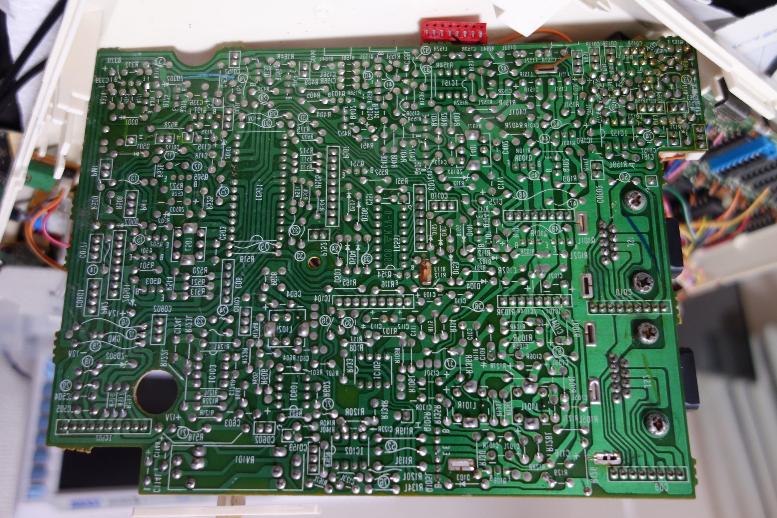
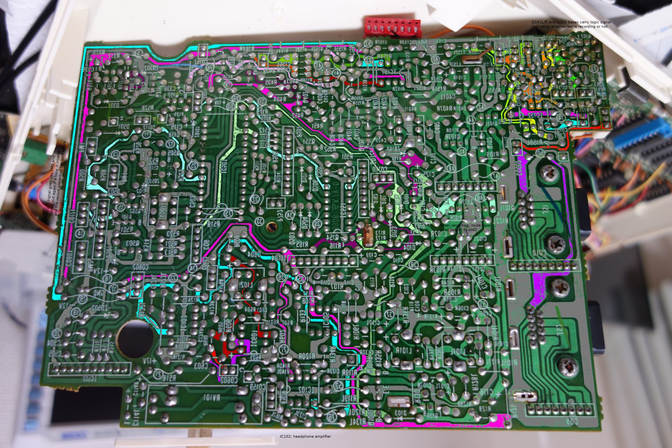
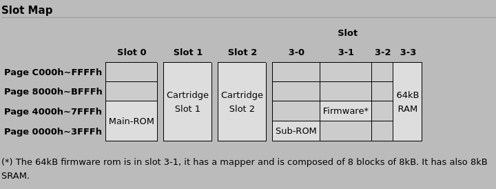
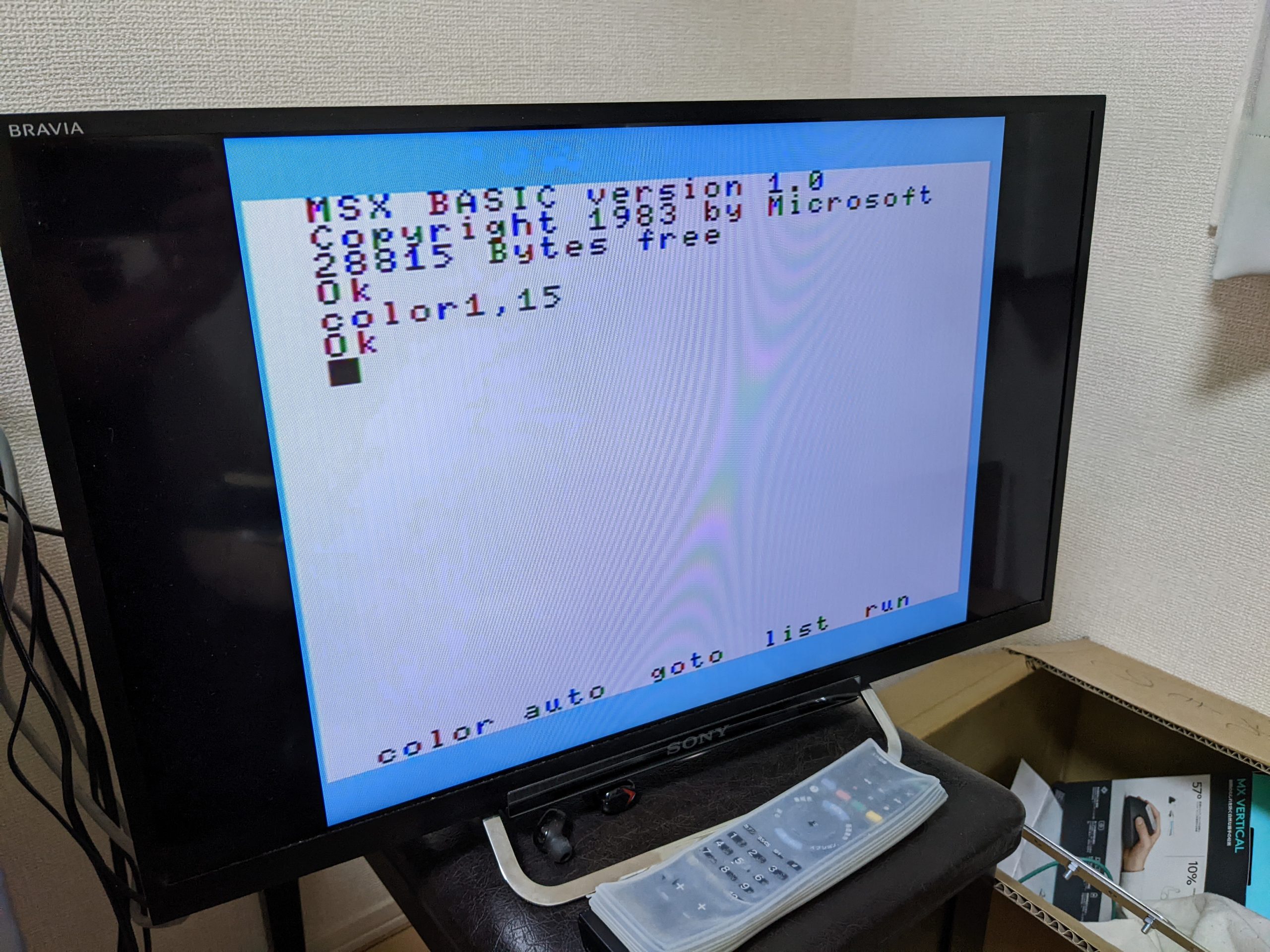
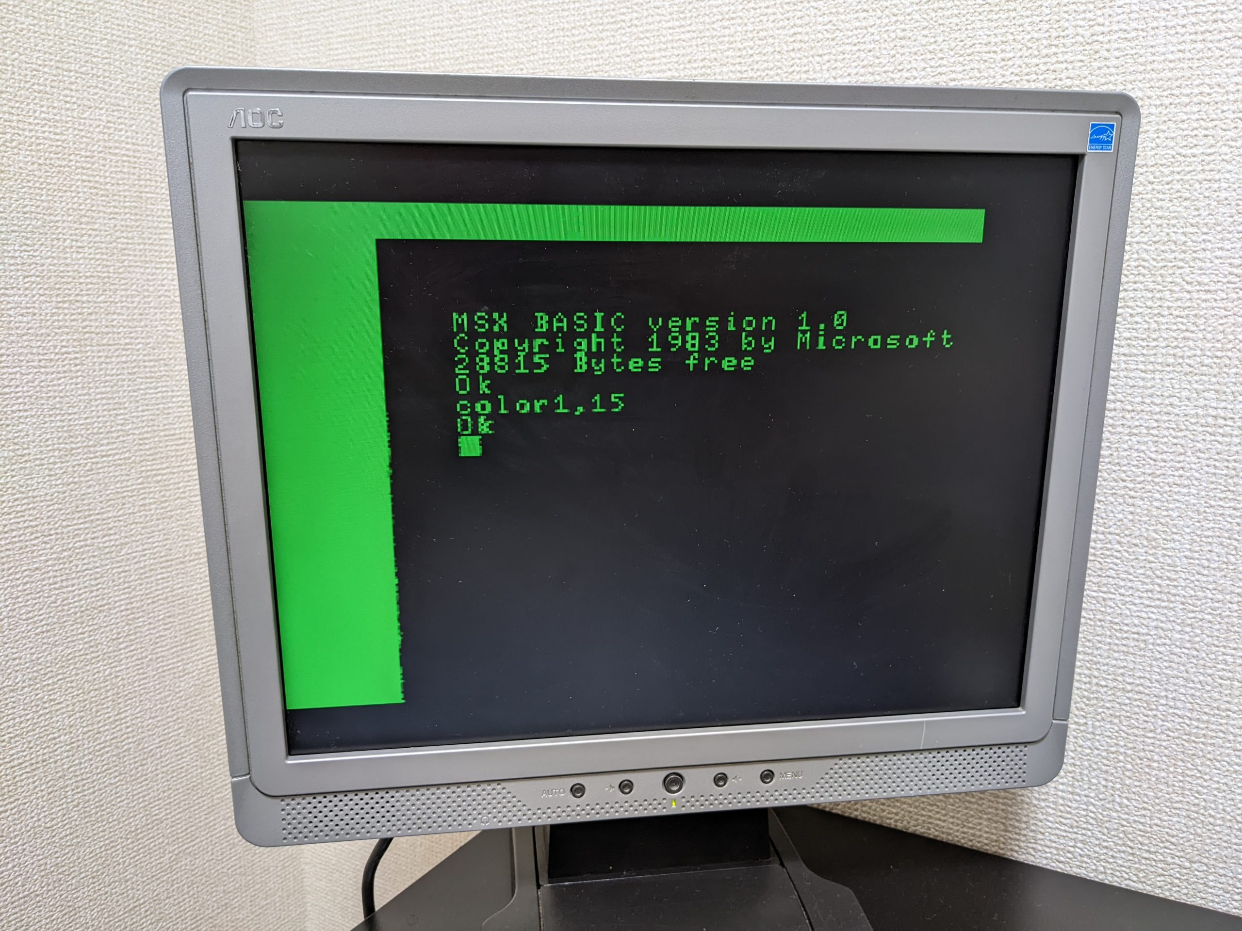
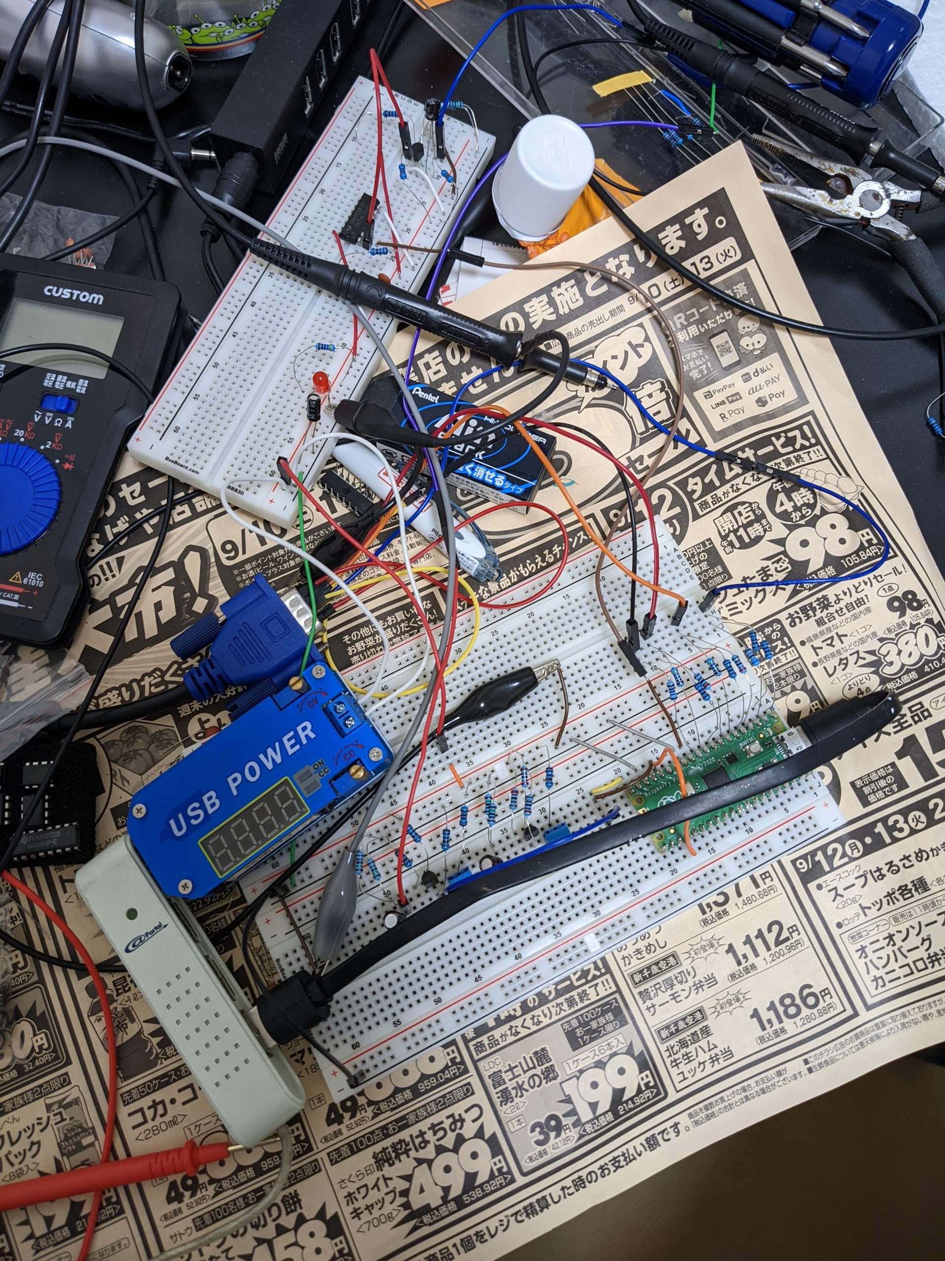

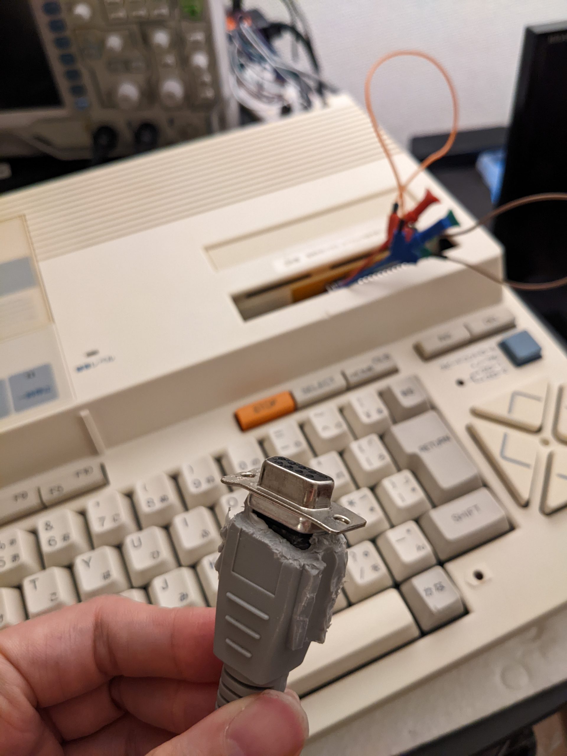
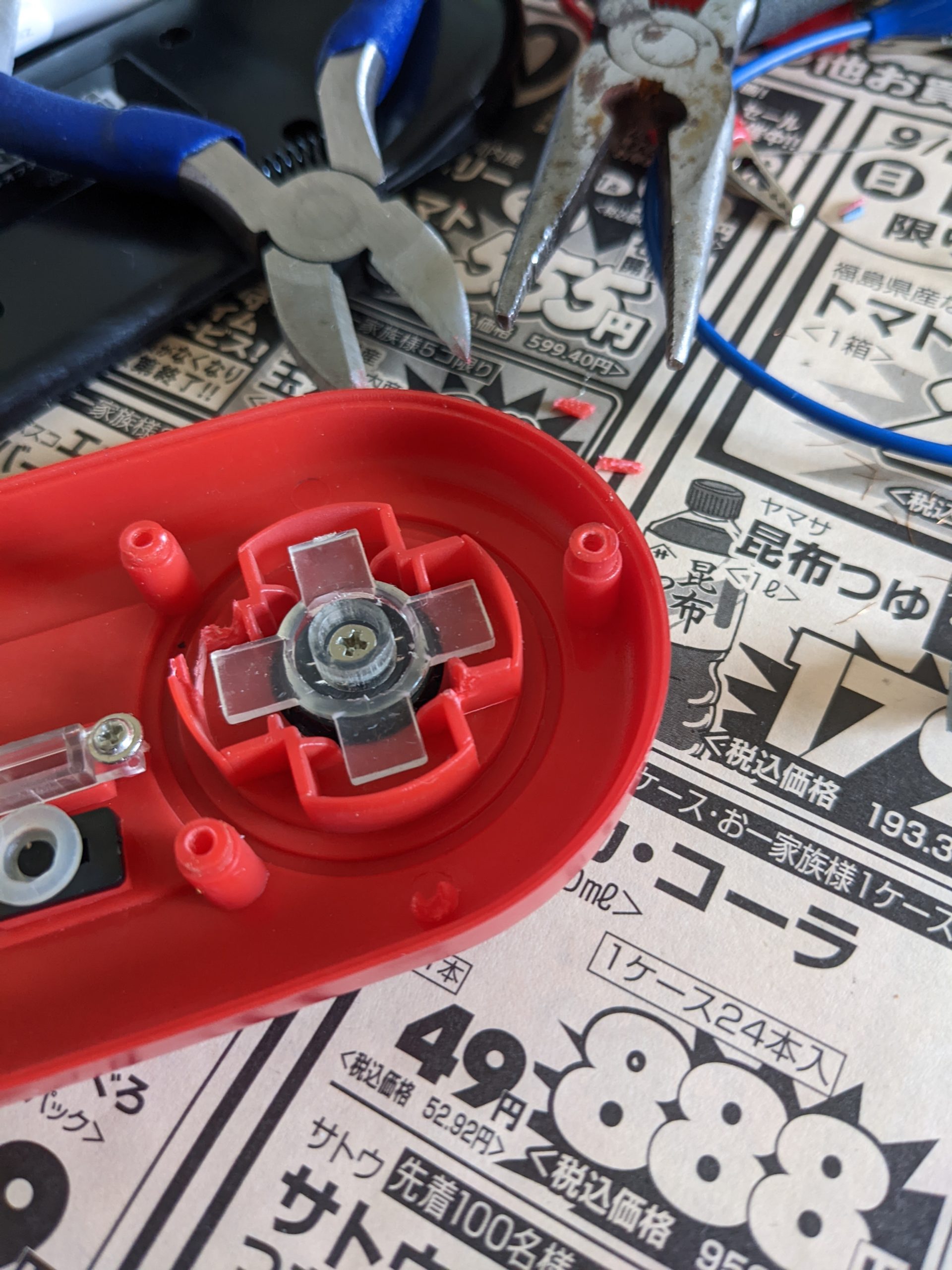
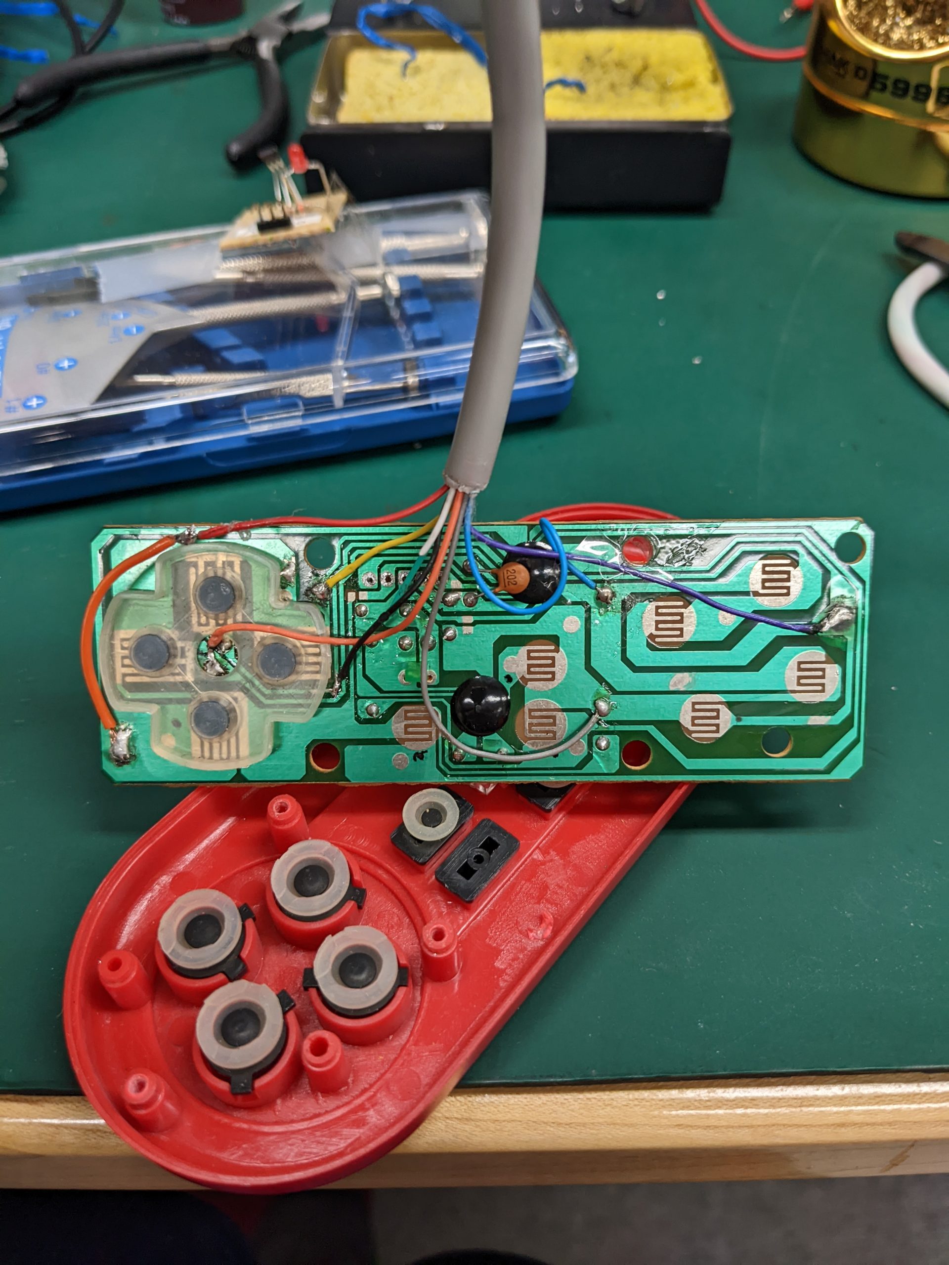
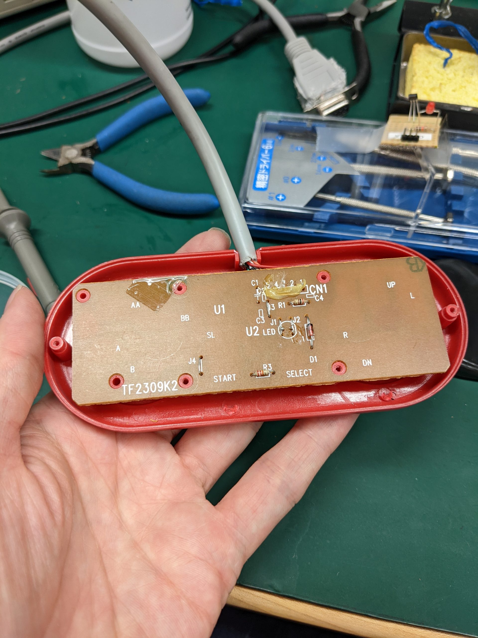

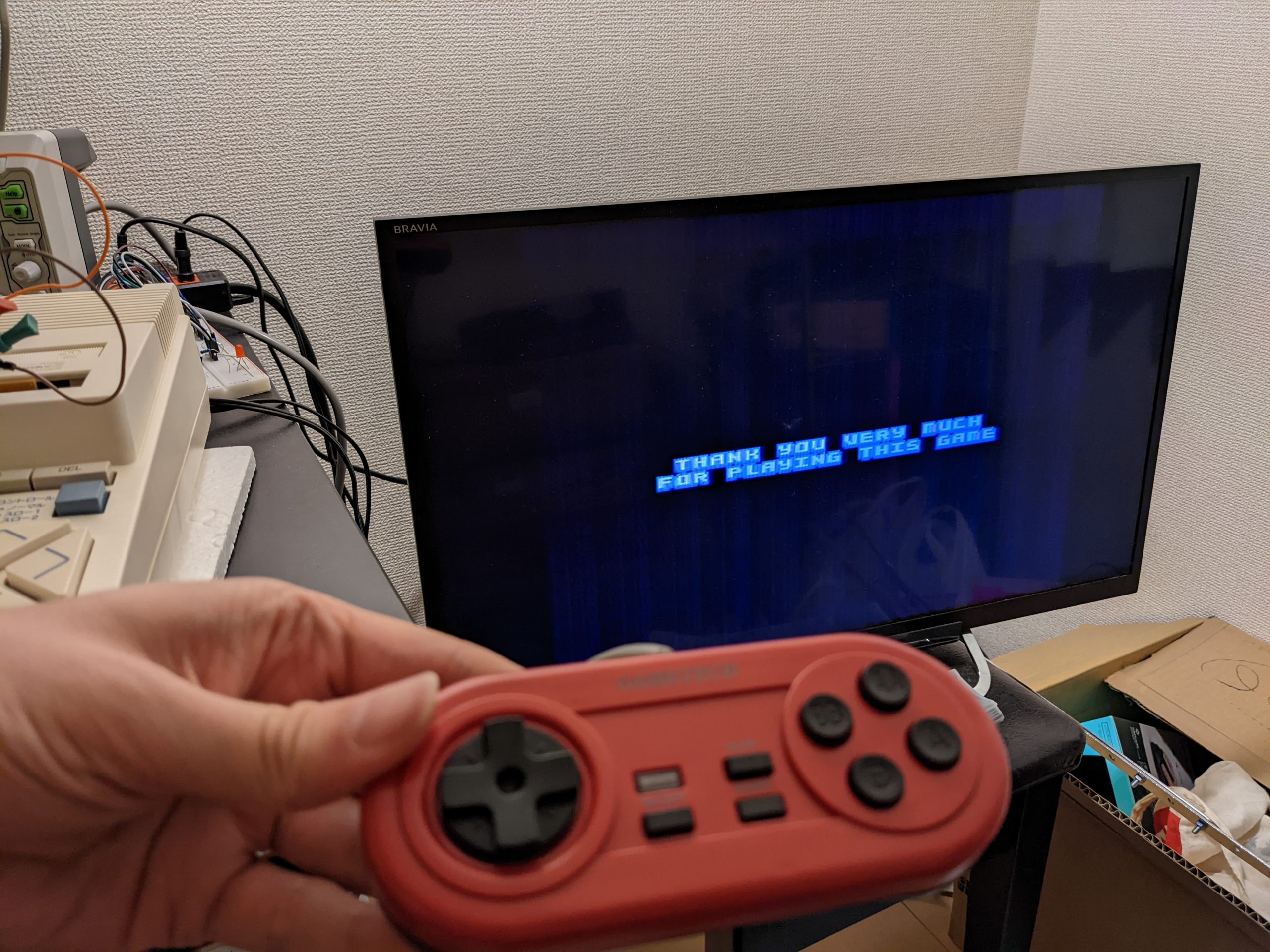
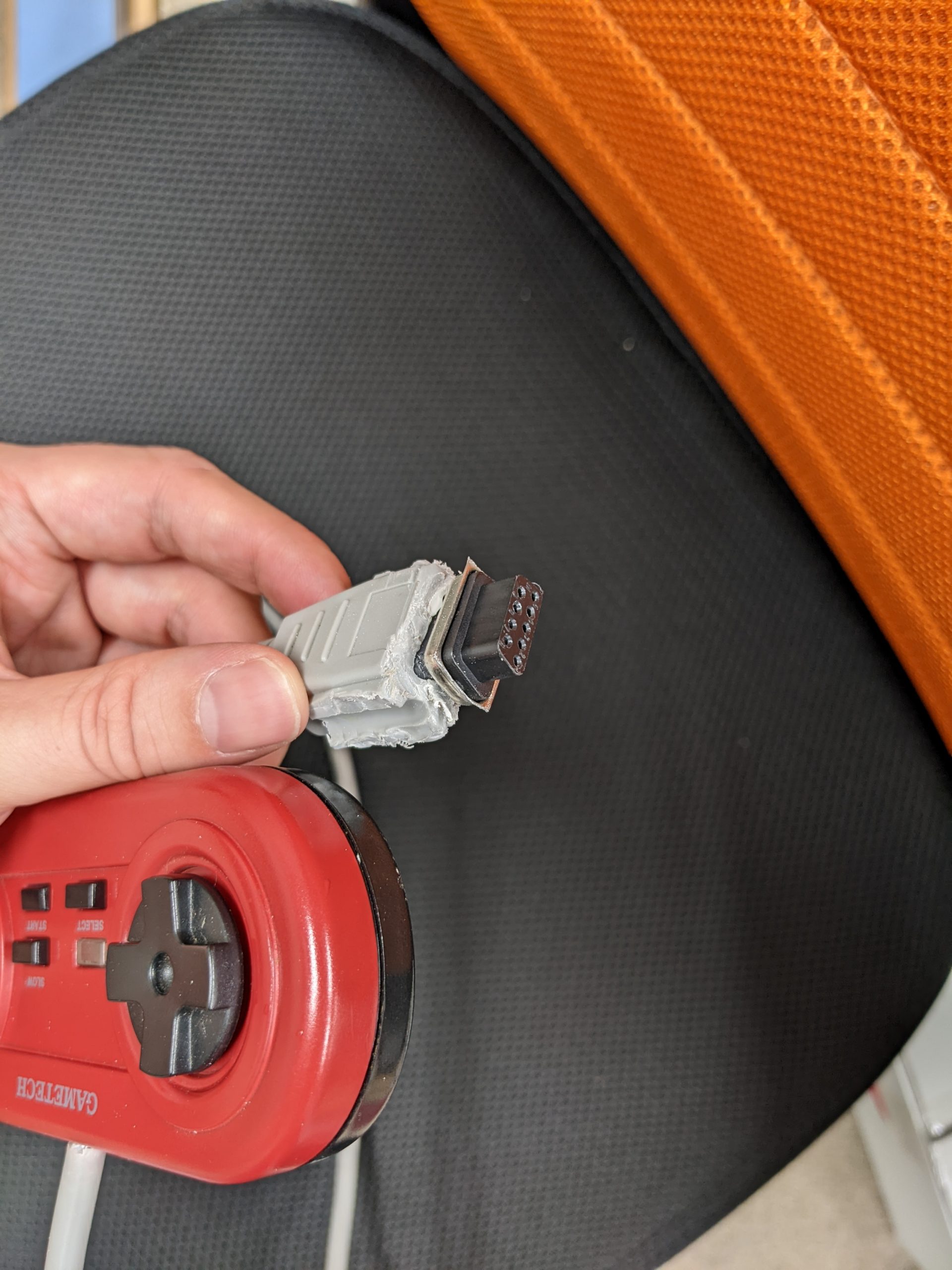
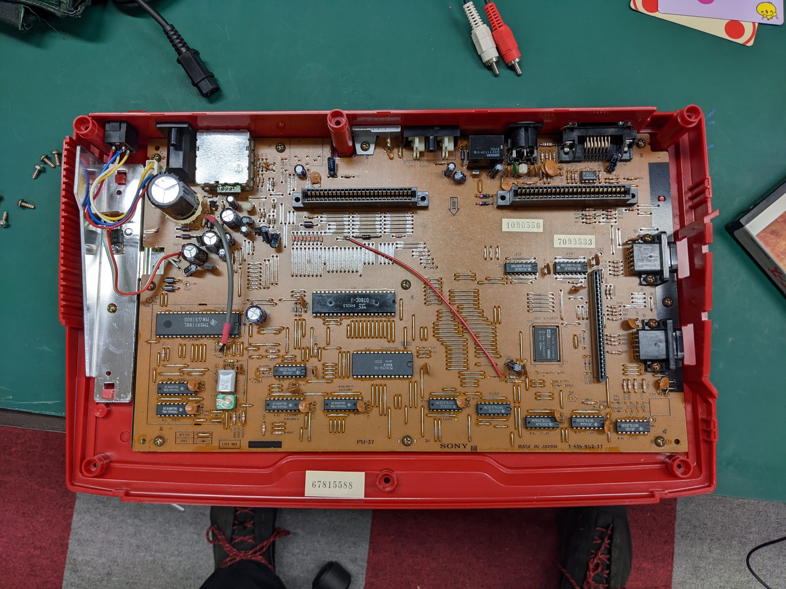

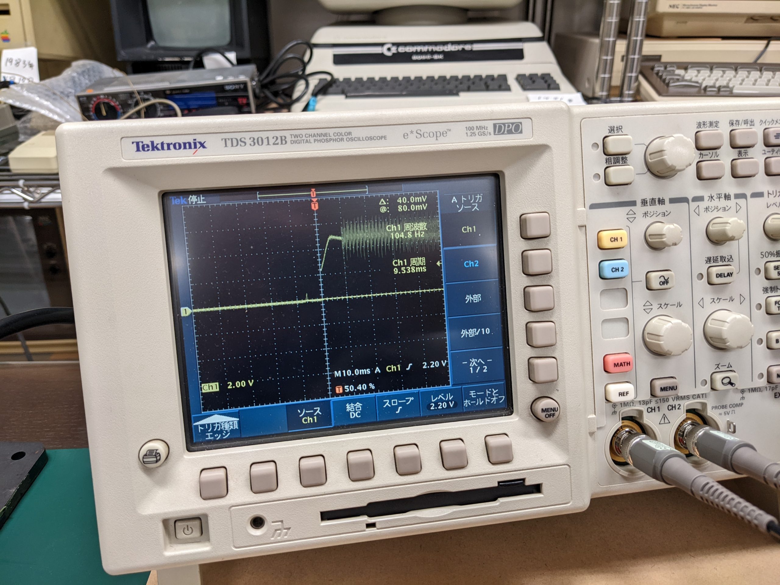
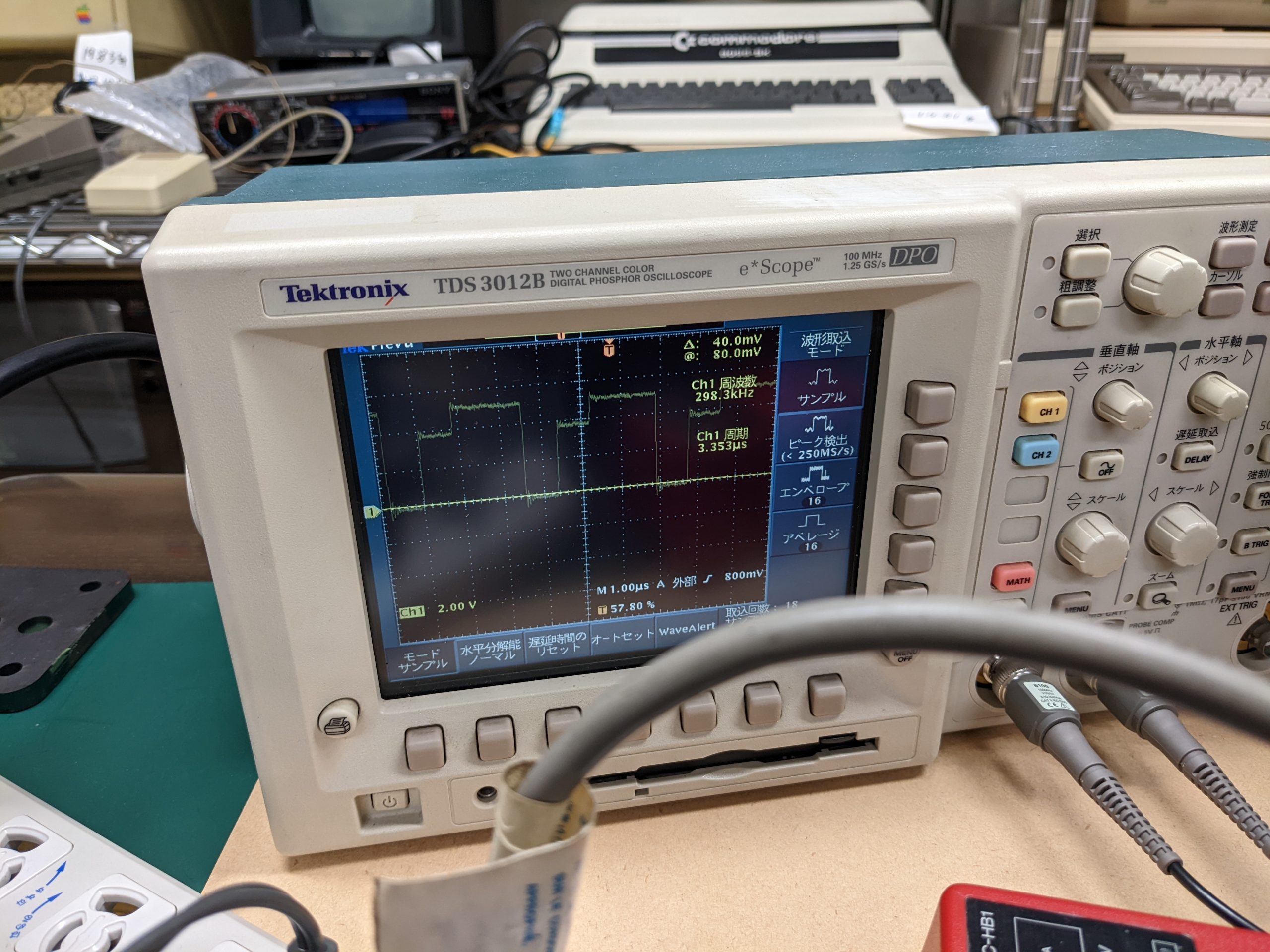
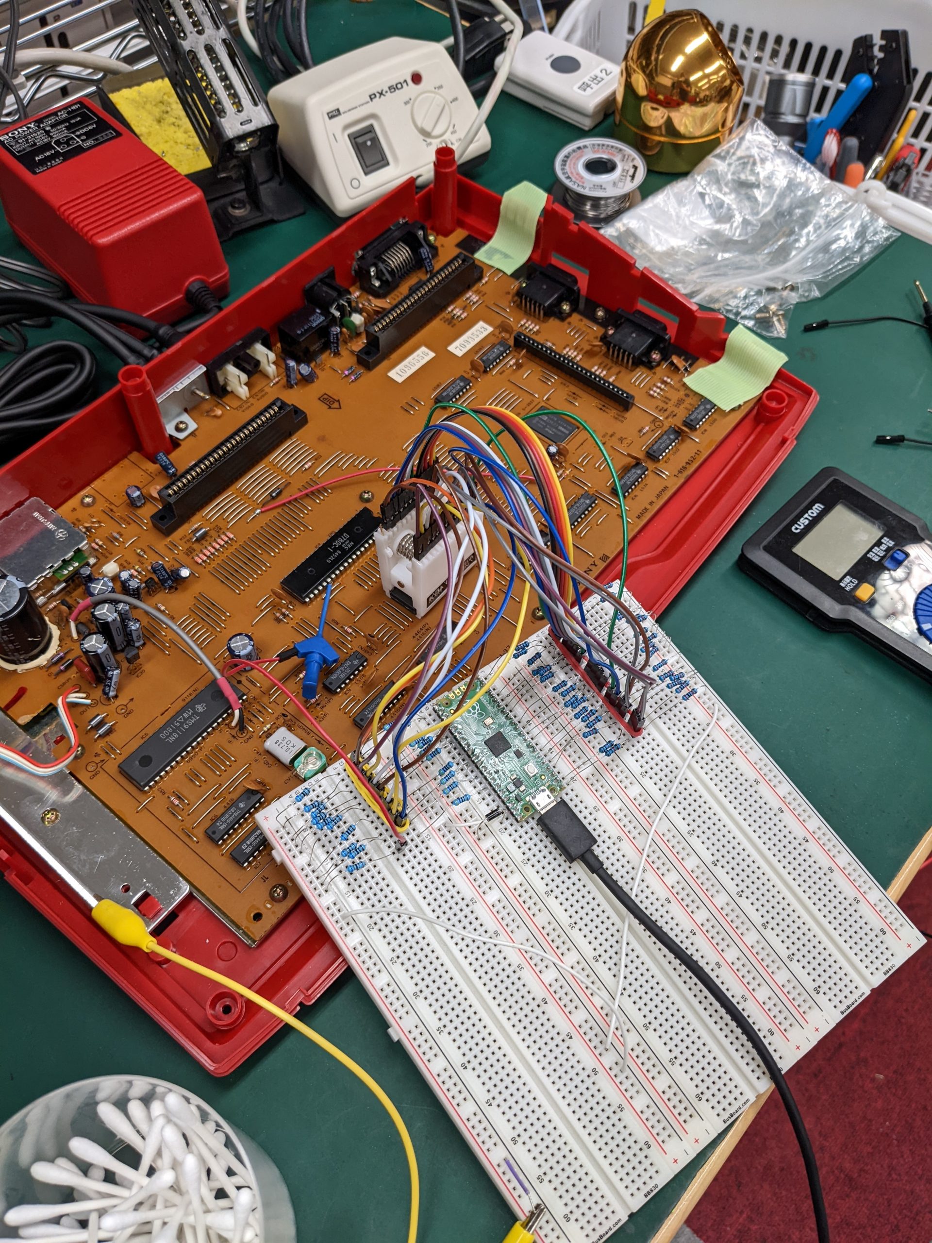
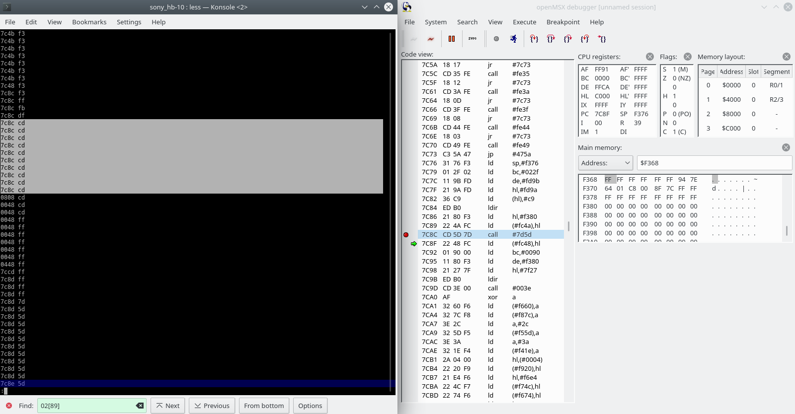
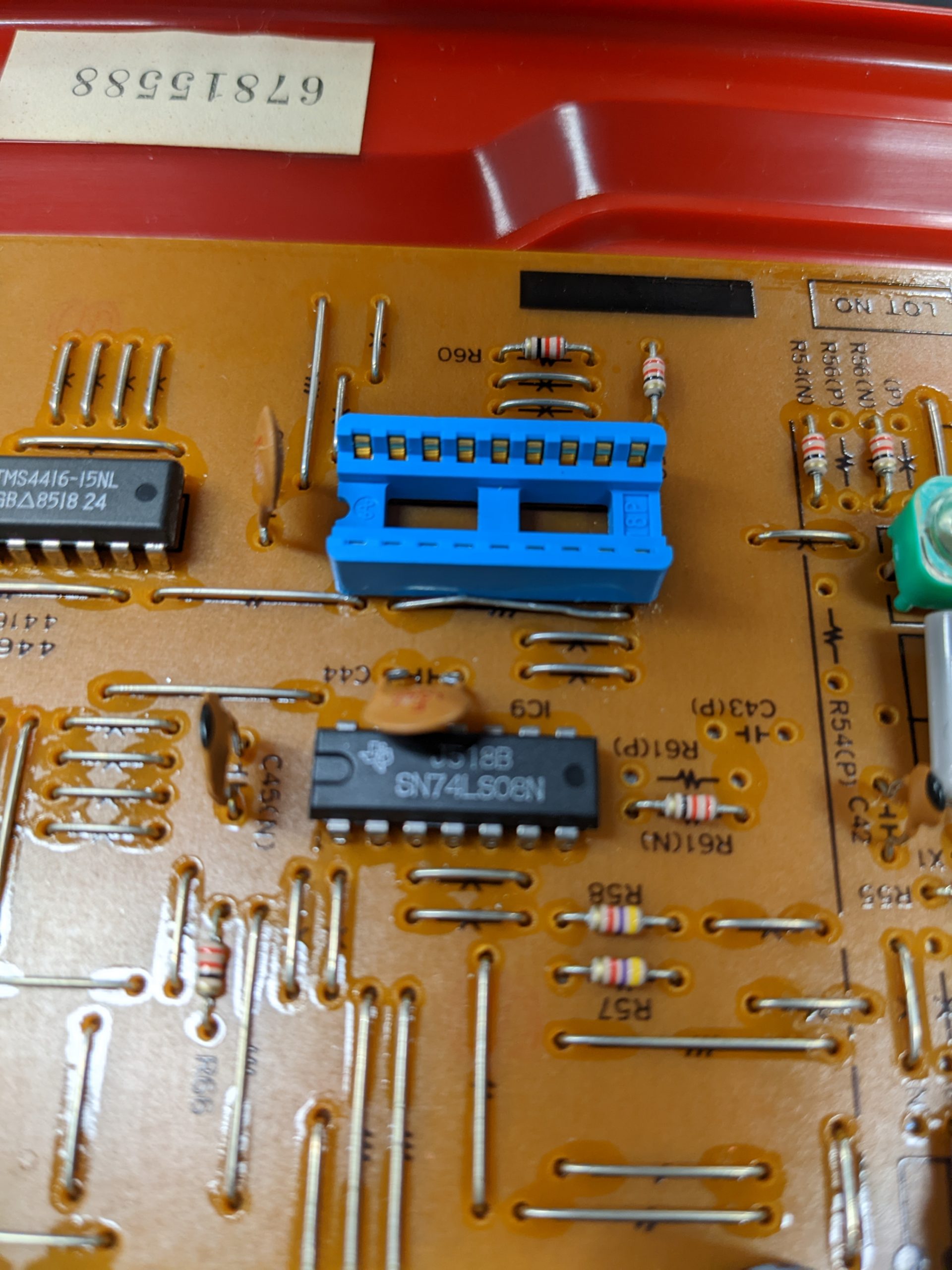


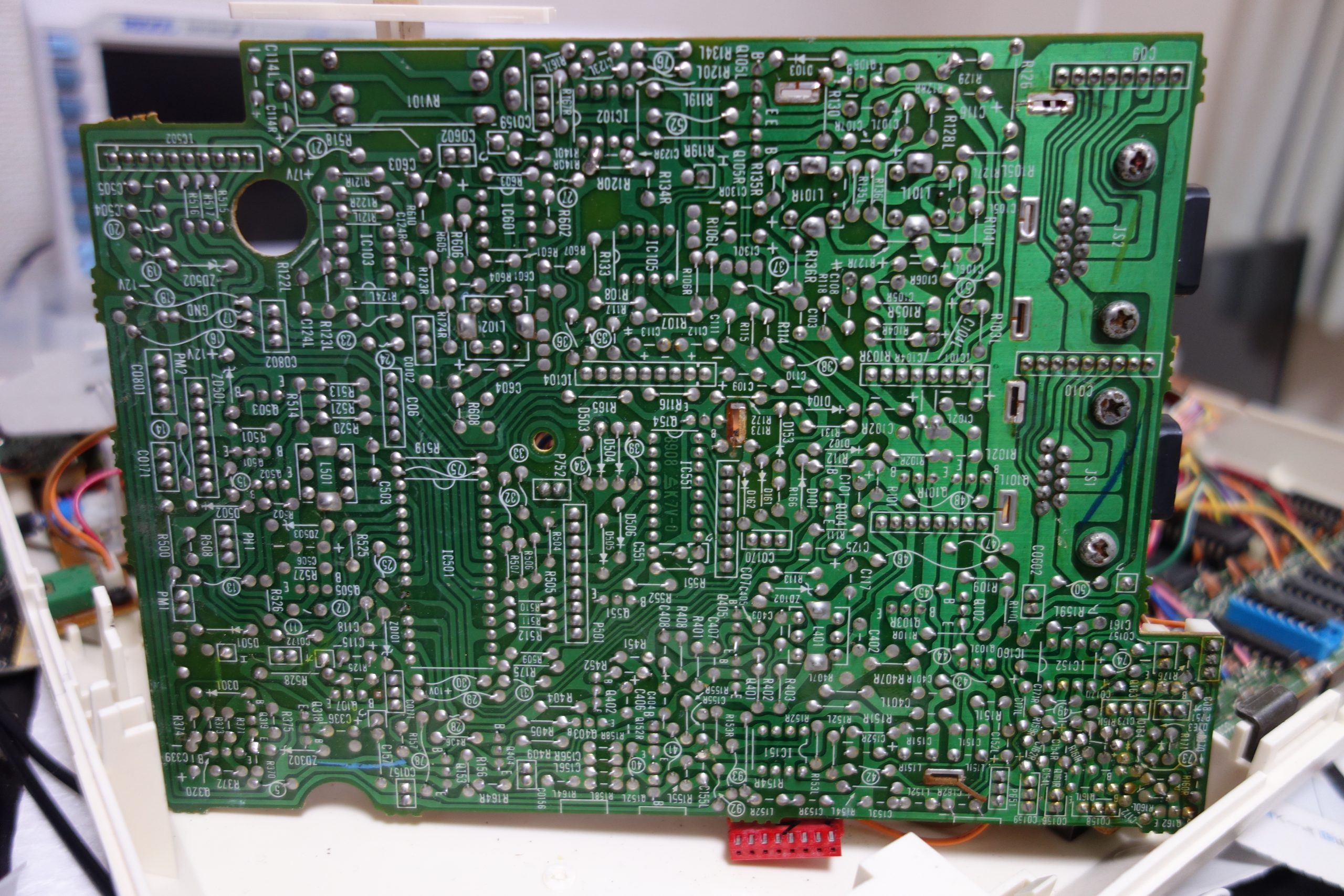
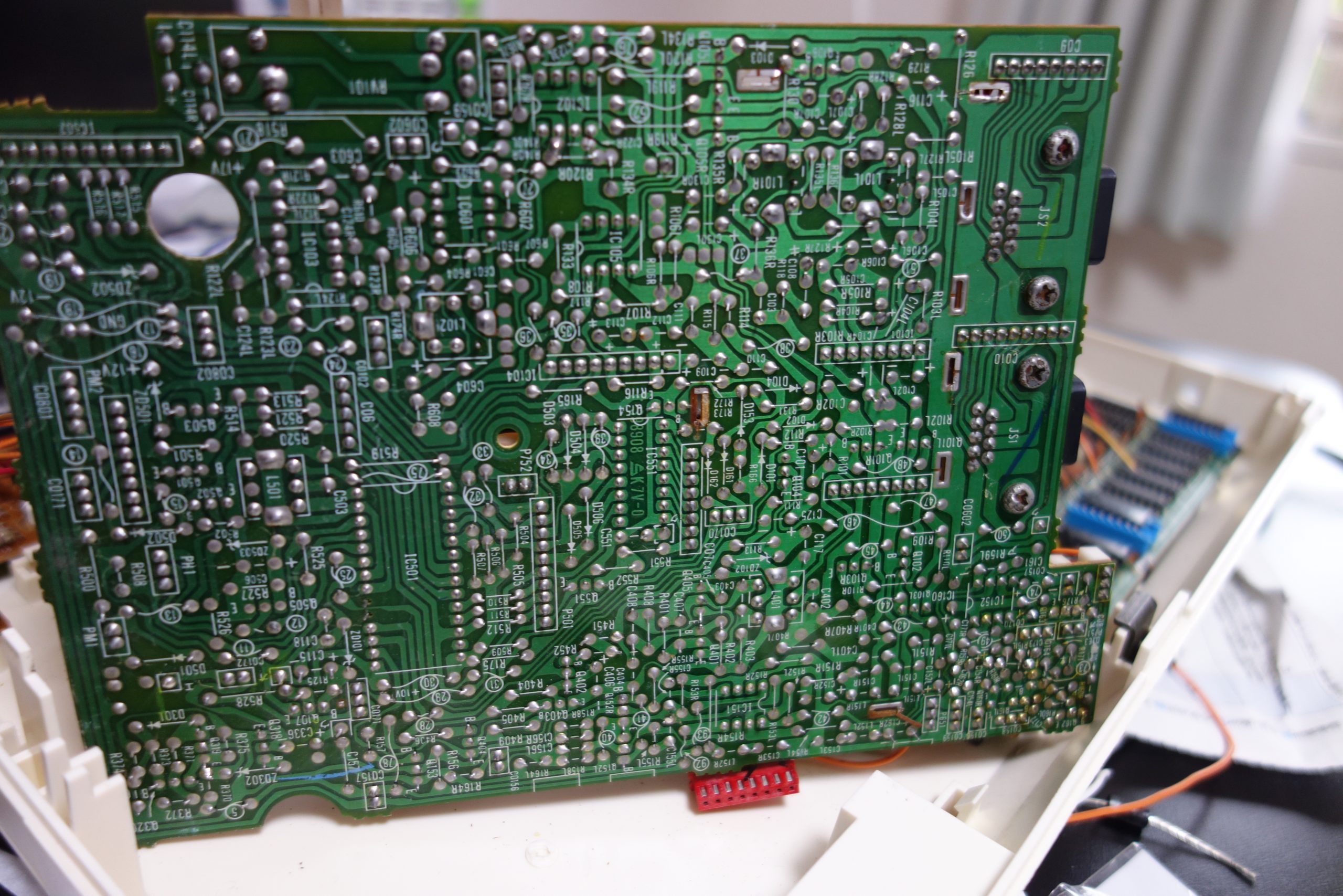
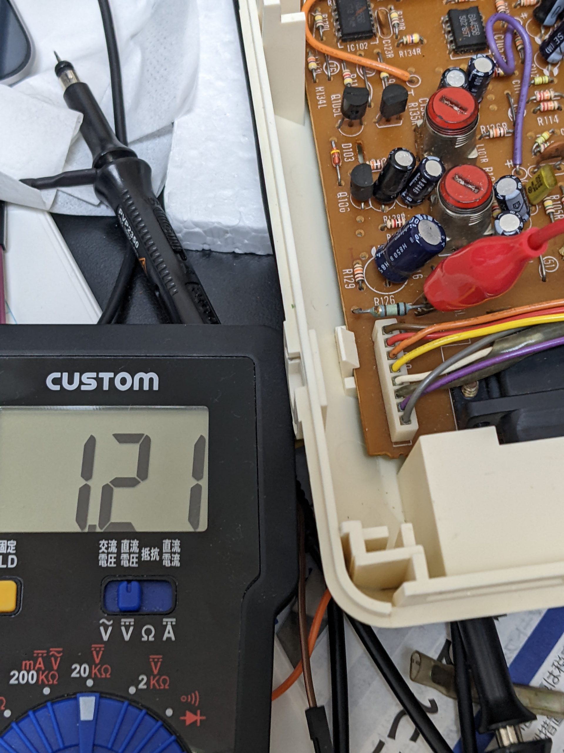
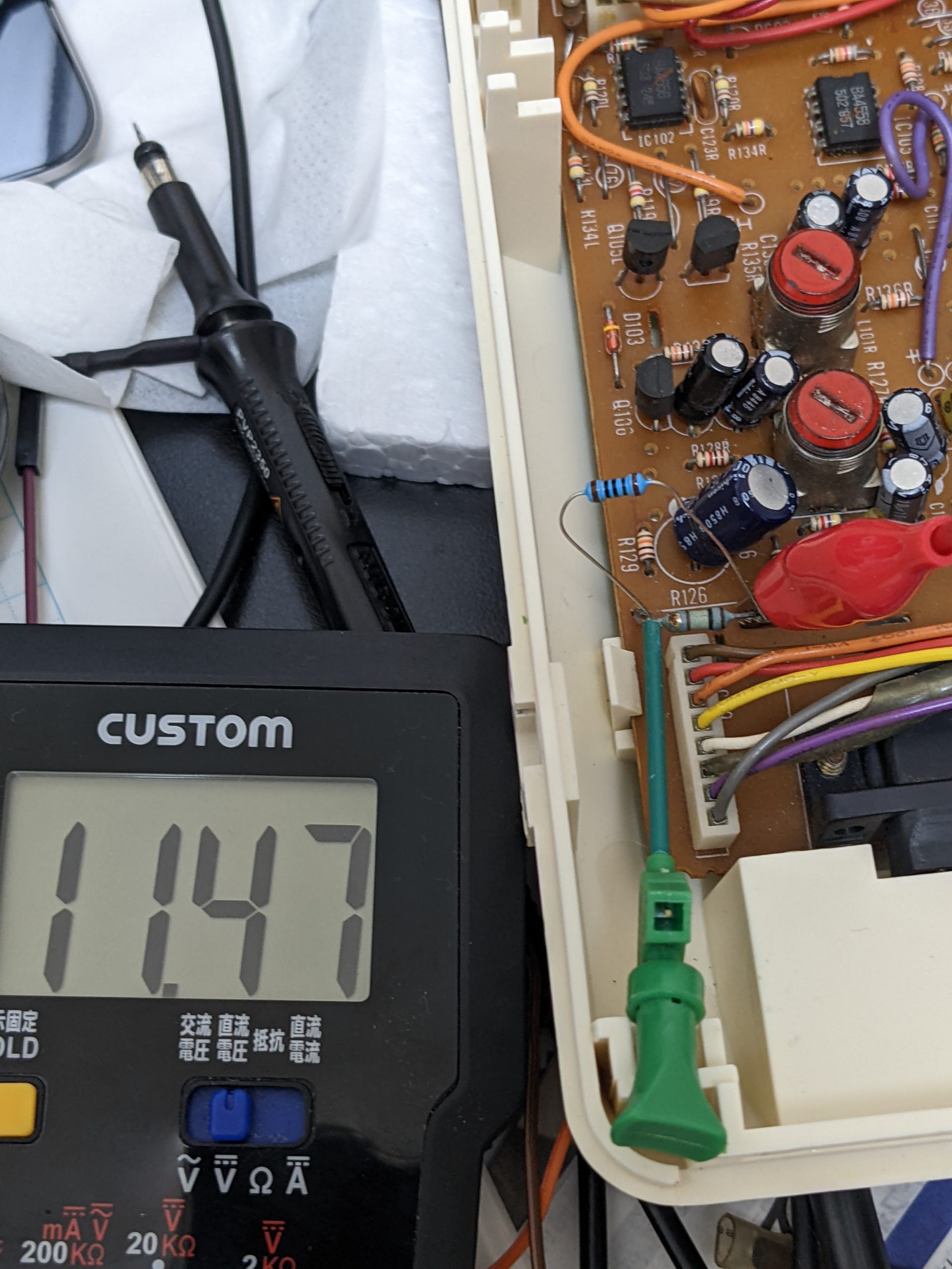
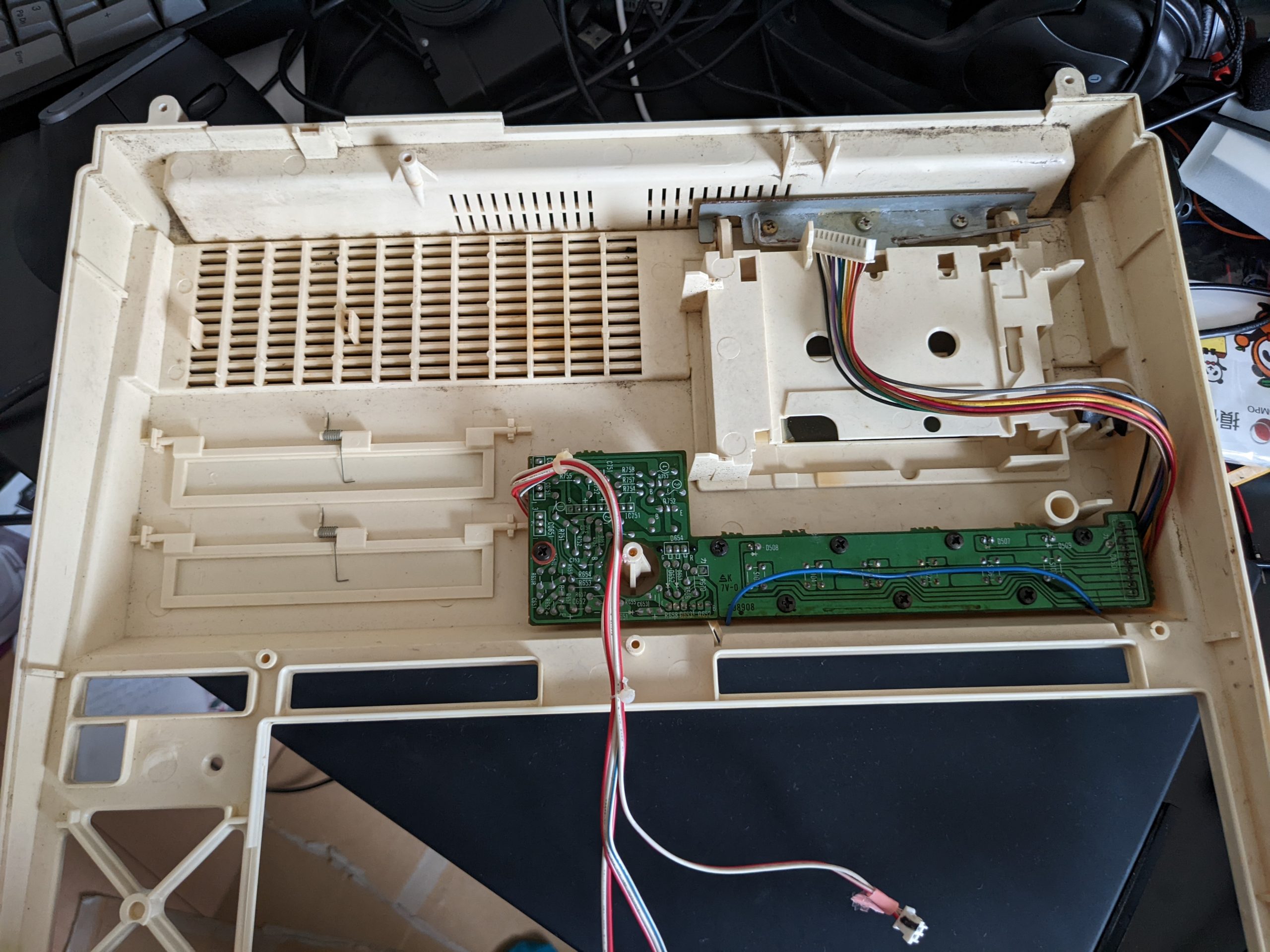

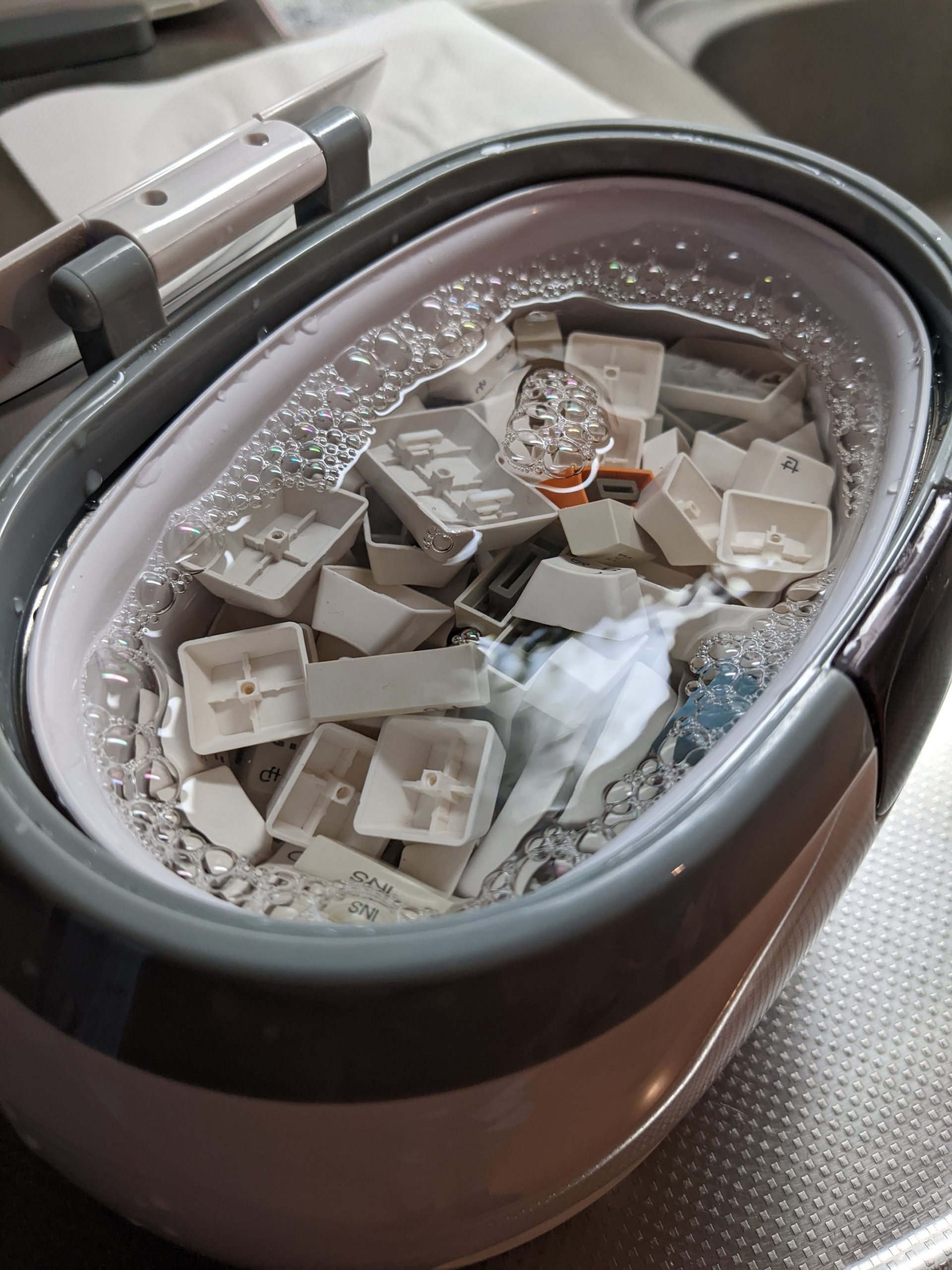
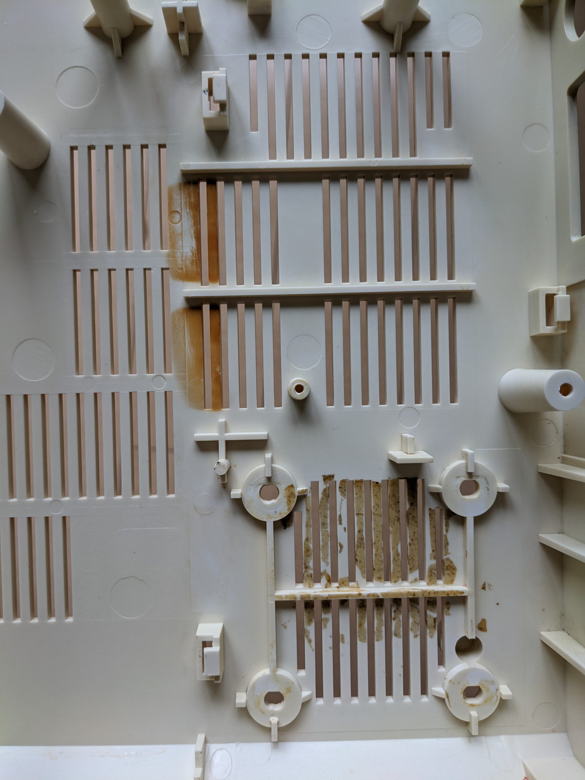

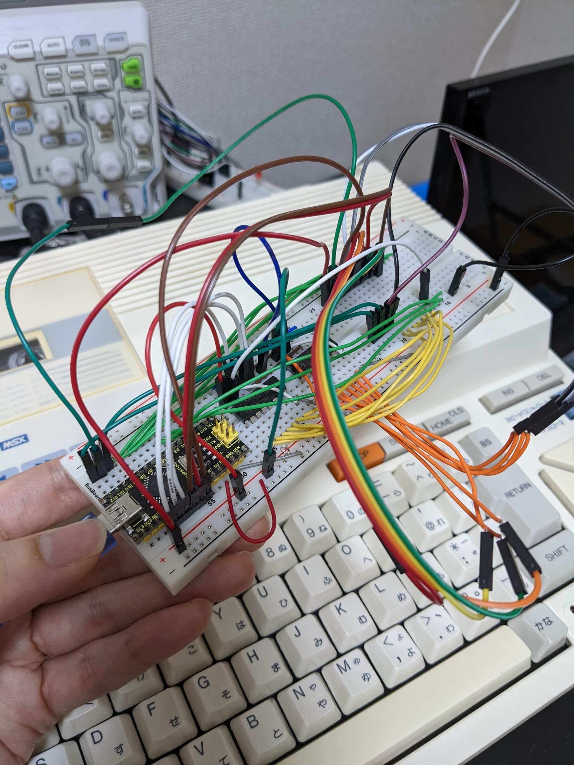
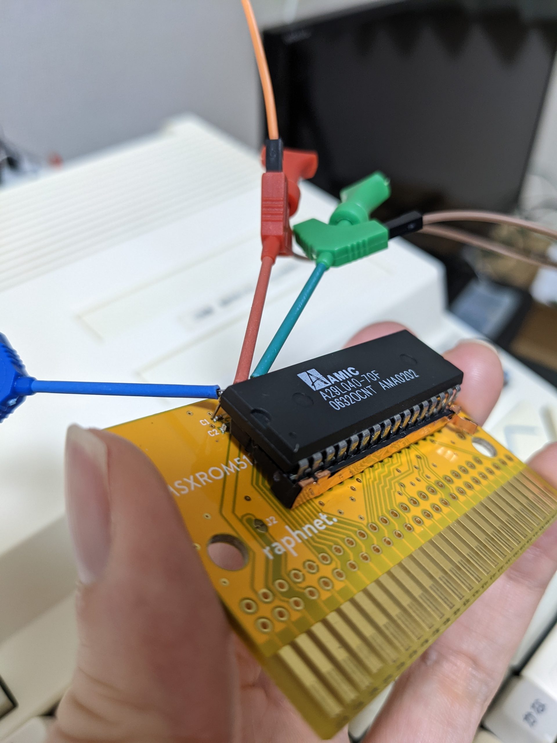
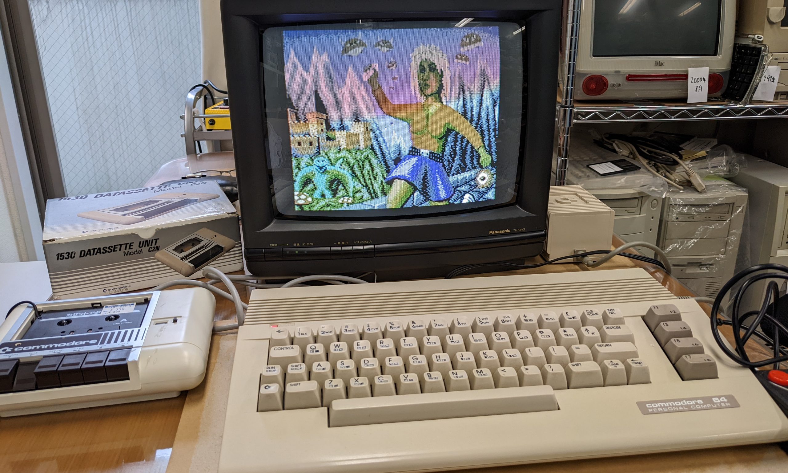
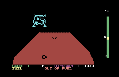

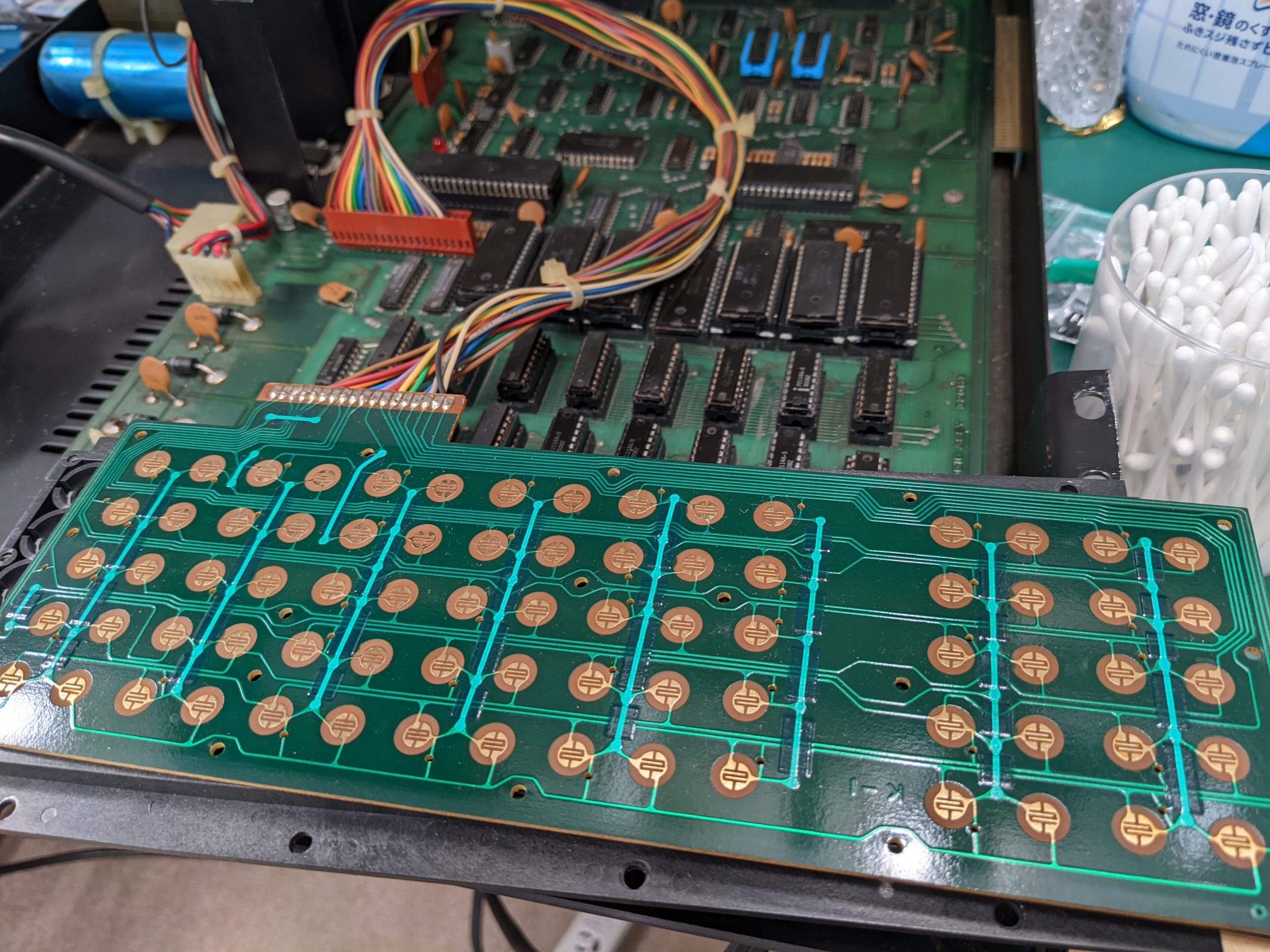
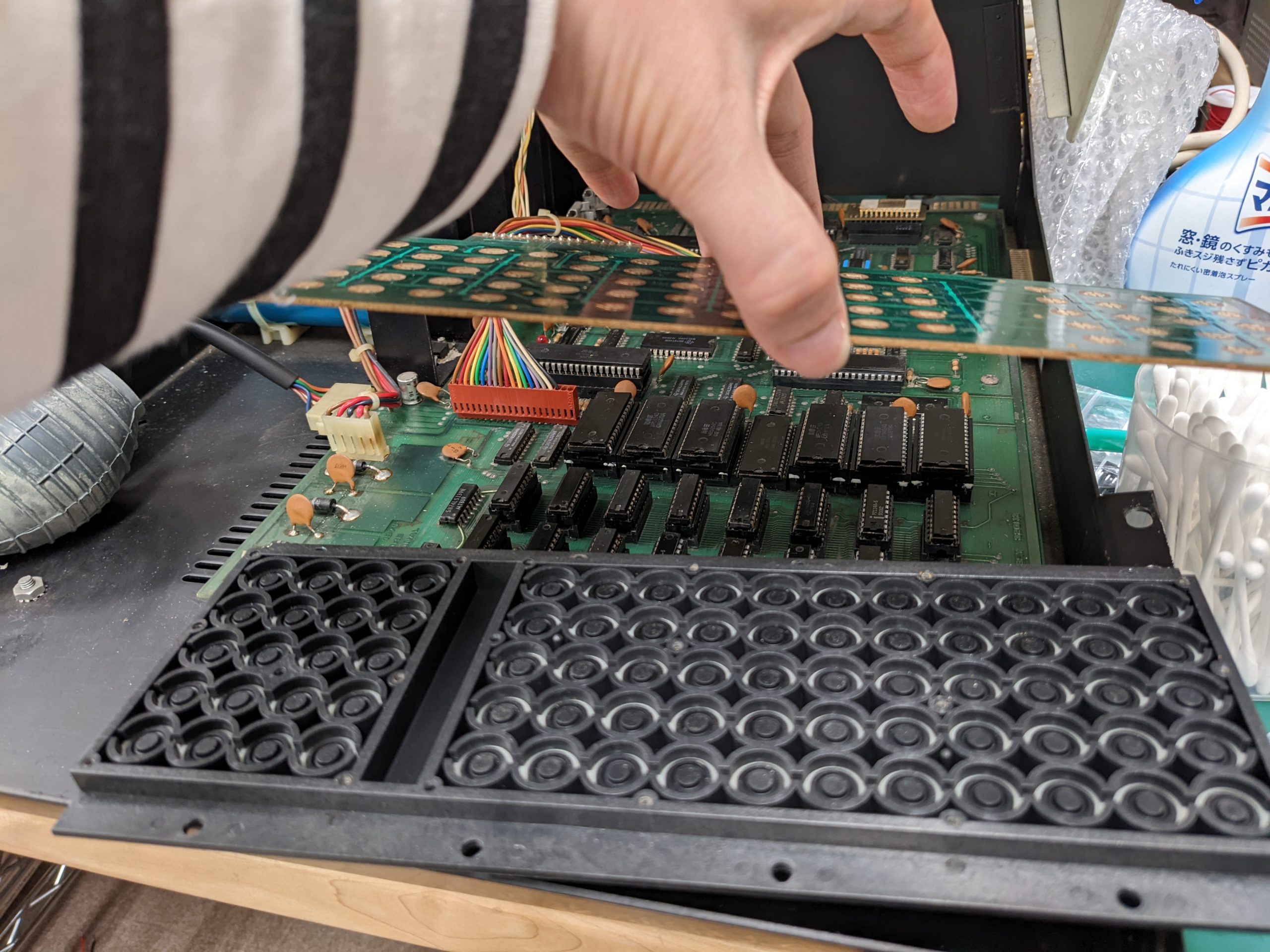
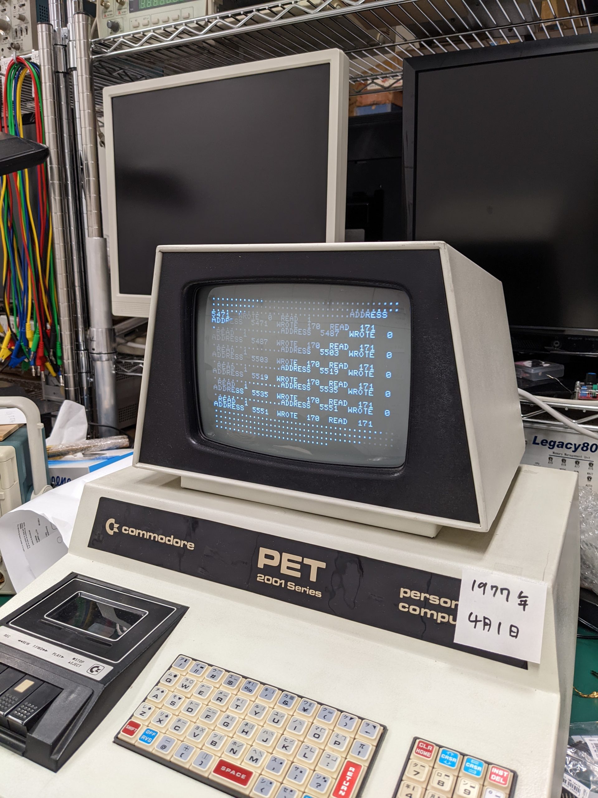
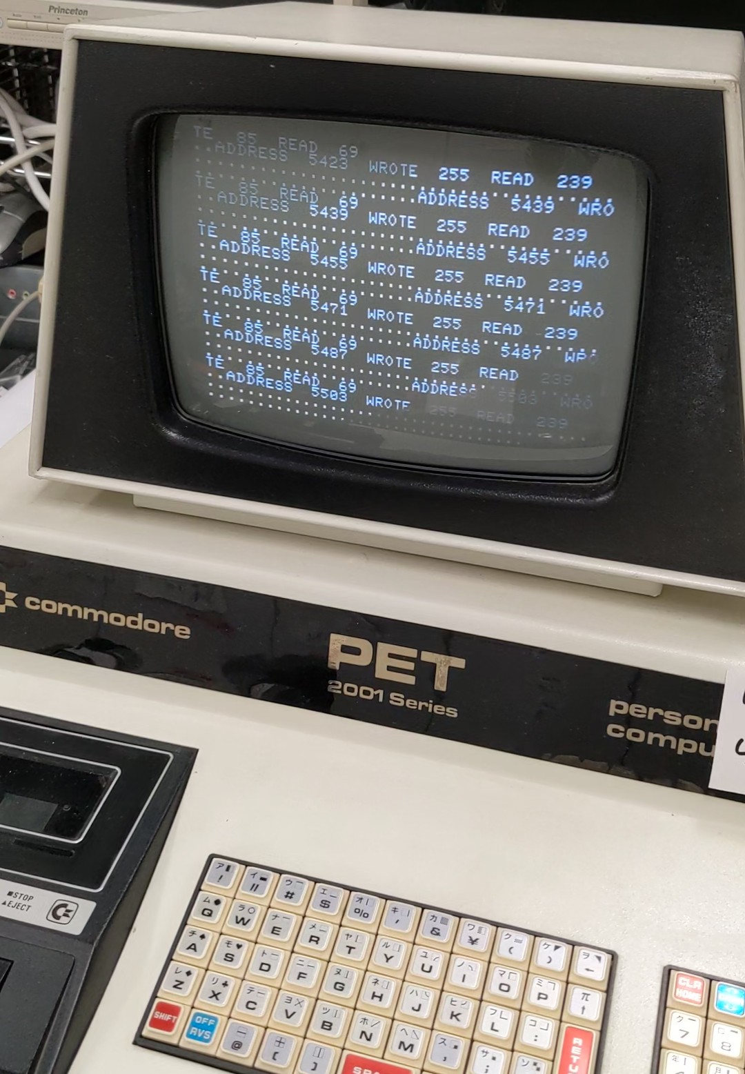
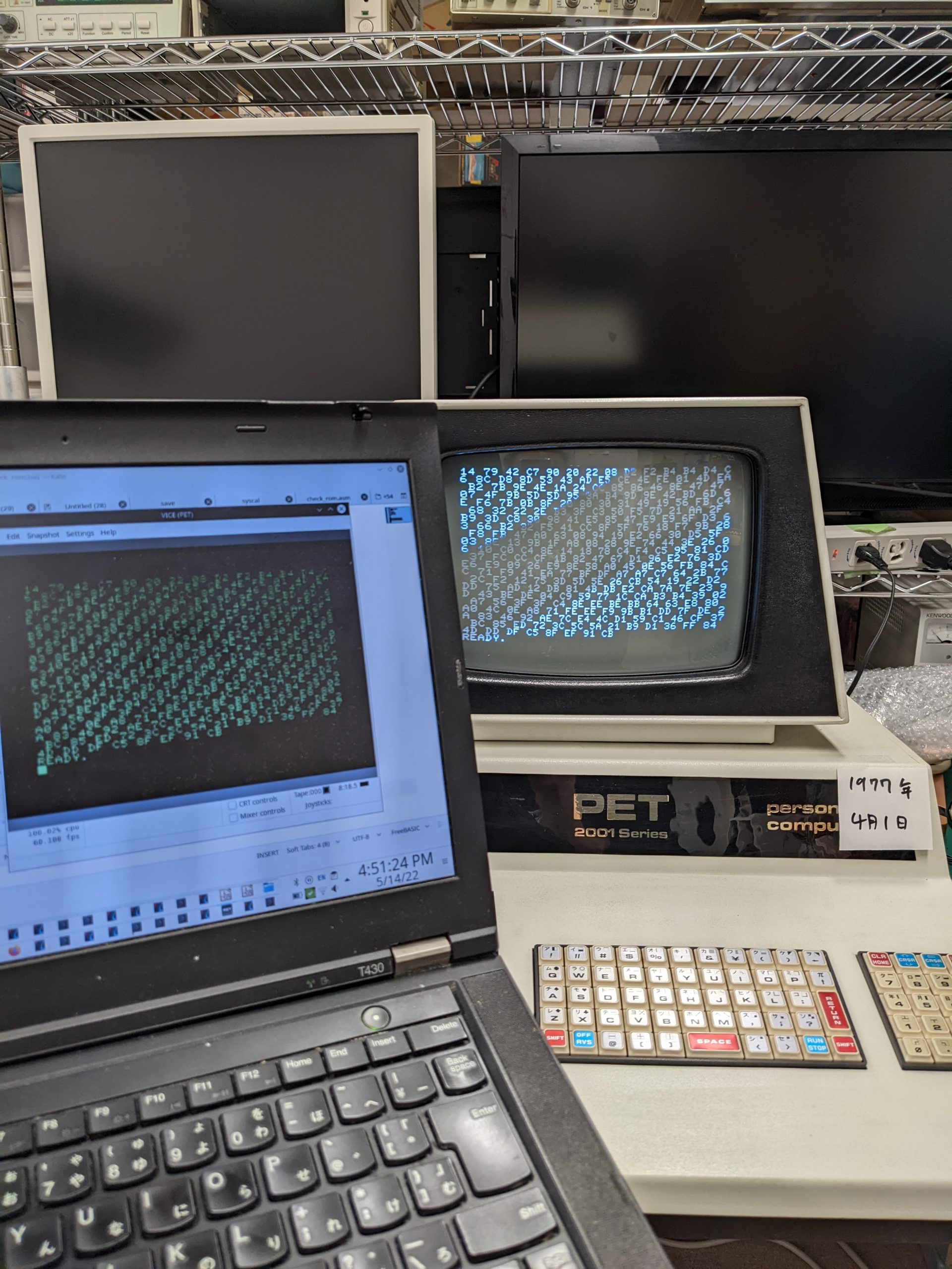
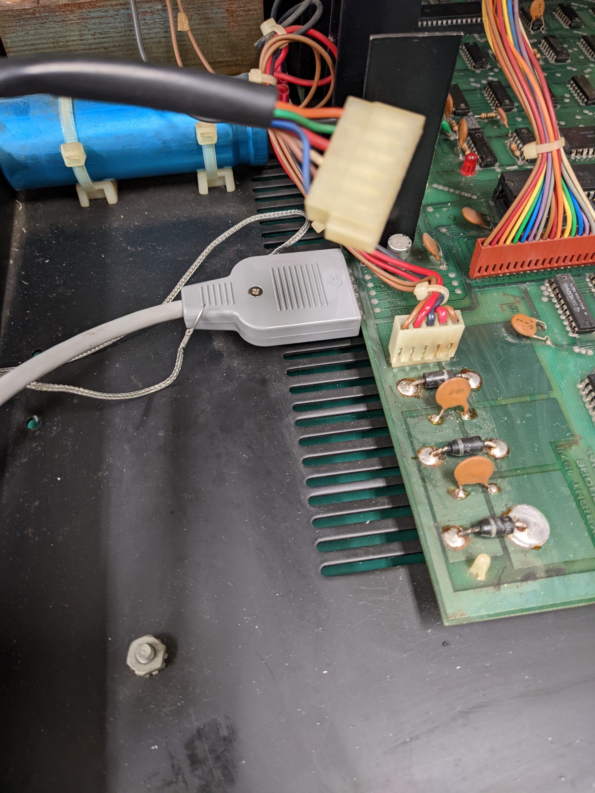
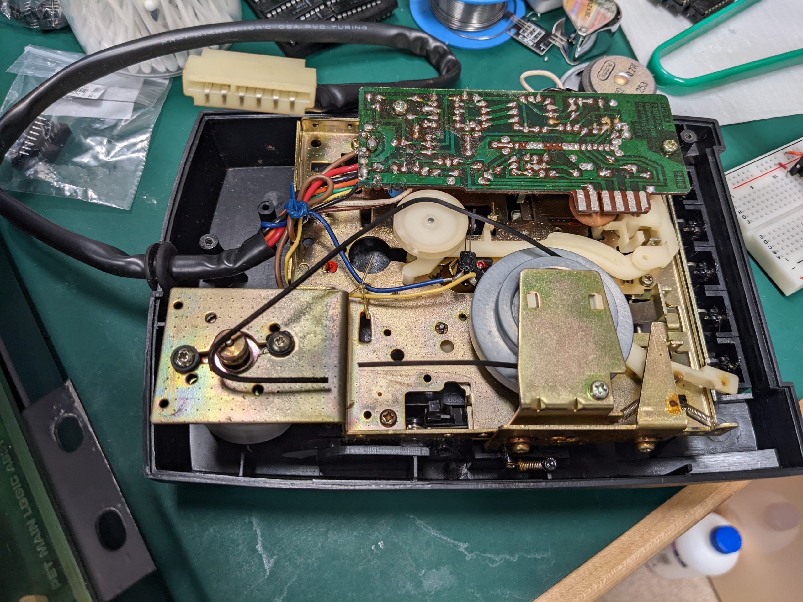
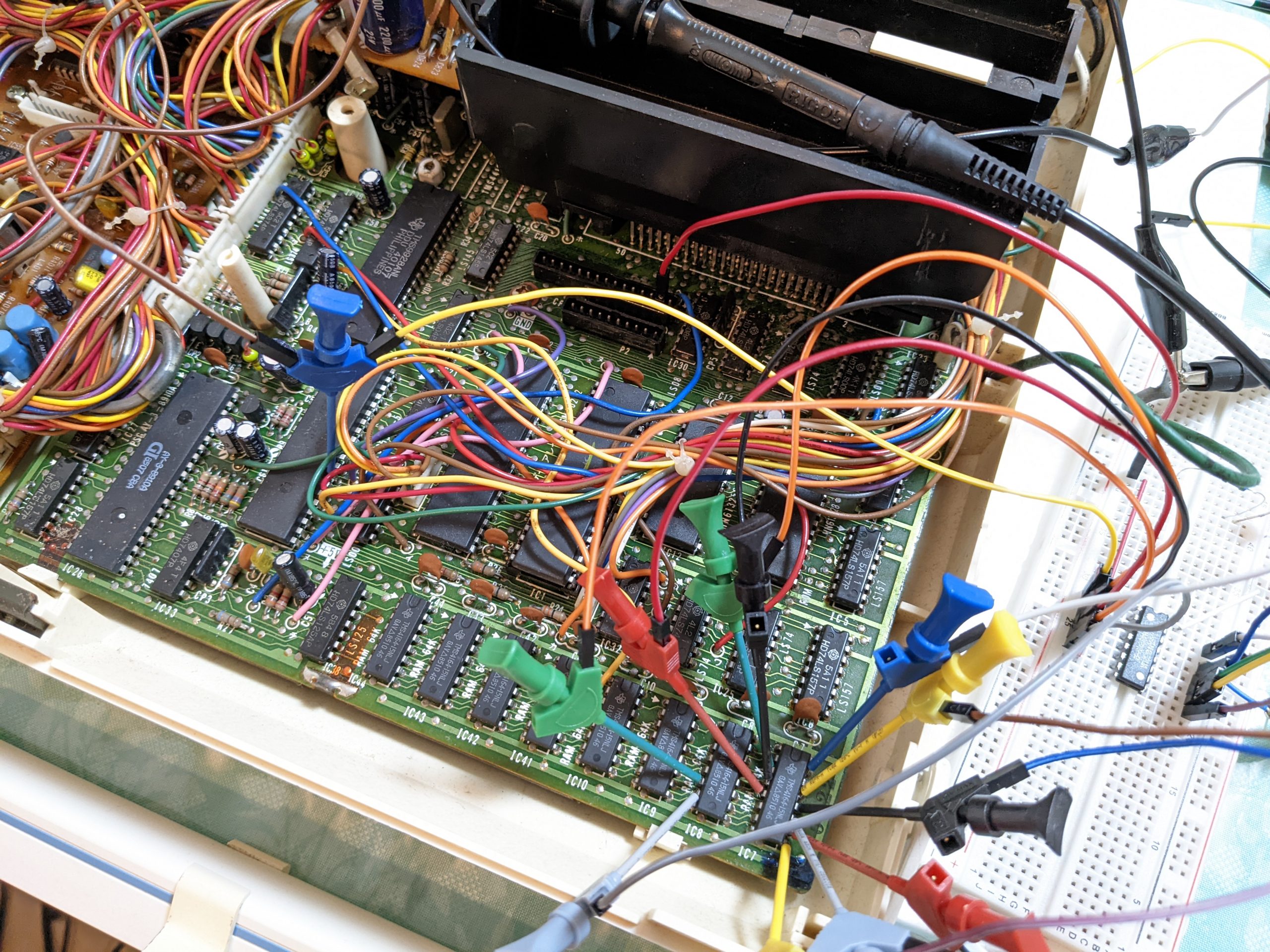
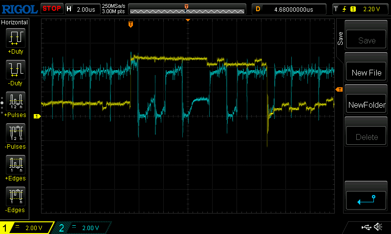
