For a quick overview of what I did to the ZX81 before arriving at this point, see this post: ZX81 repair (no video, some keys not working, and bad RAM pack)
I recently got hold of a Spectrum ZX81 RAM pack that when plugged in, produced a garbled screen on boot. I decided to check what’s wrong before ordering any chips. To do that, I first looked at the schematics and made sure there were no bad connections. This was a laborious process, but fortunately all RAM chips share all pins except the data pins, so you should have continuity between all pins except two on all RAM chips.
I finally thought I found something broken — but it turned out that there’s just a slight difference between my board and the schematics: only three NAND gates are used on the quad NAND IC, and logically and electrically it doesn’t matter which gates you use and which one you leave unsoldered. Well, for some reason my board used different pins (i.e., left a different gate unsoldered) than the ones in the schematics.
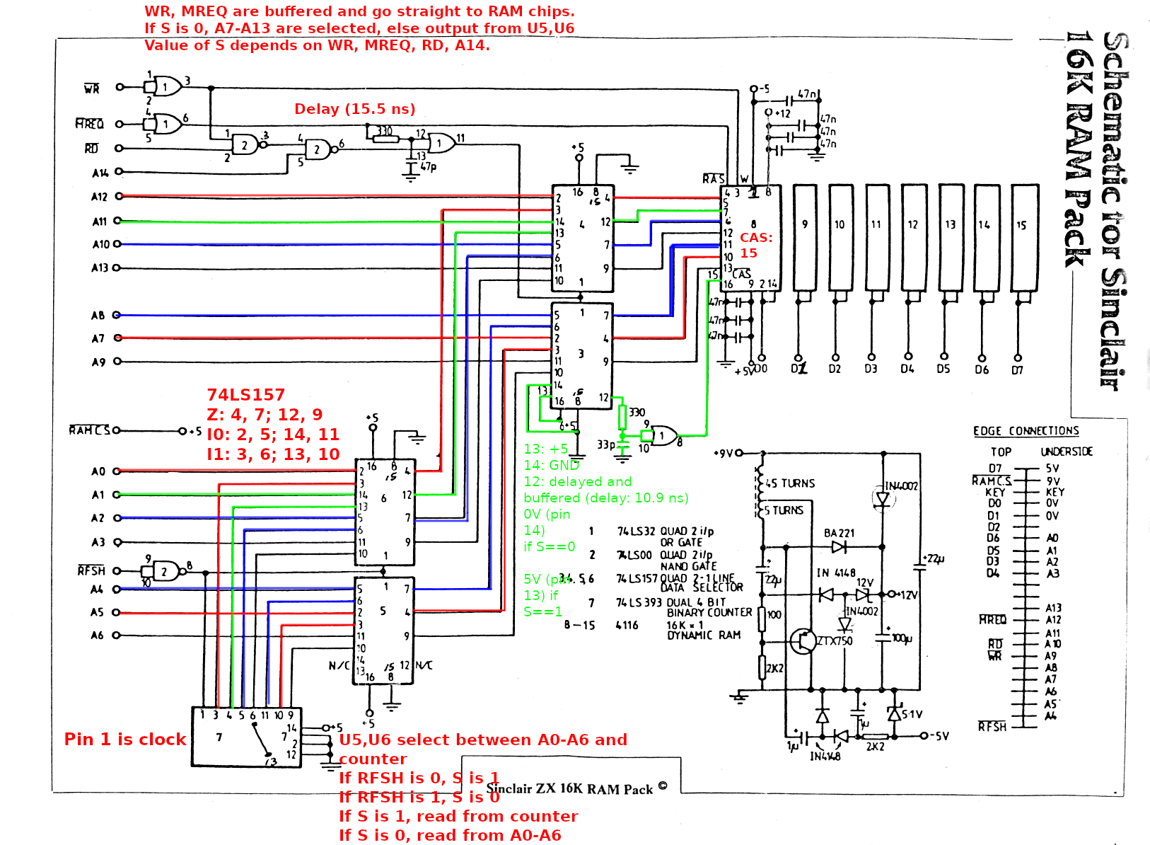
Below you will find my annotated schematics of the RAM pack.
Here is an actual picture (with the bad RAM chip replaced) that shows which chips are where:
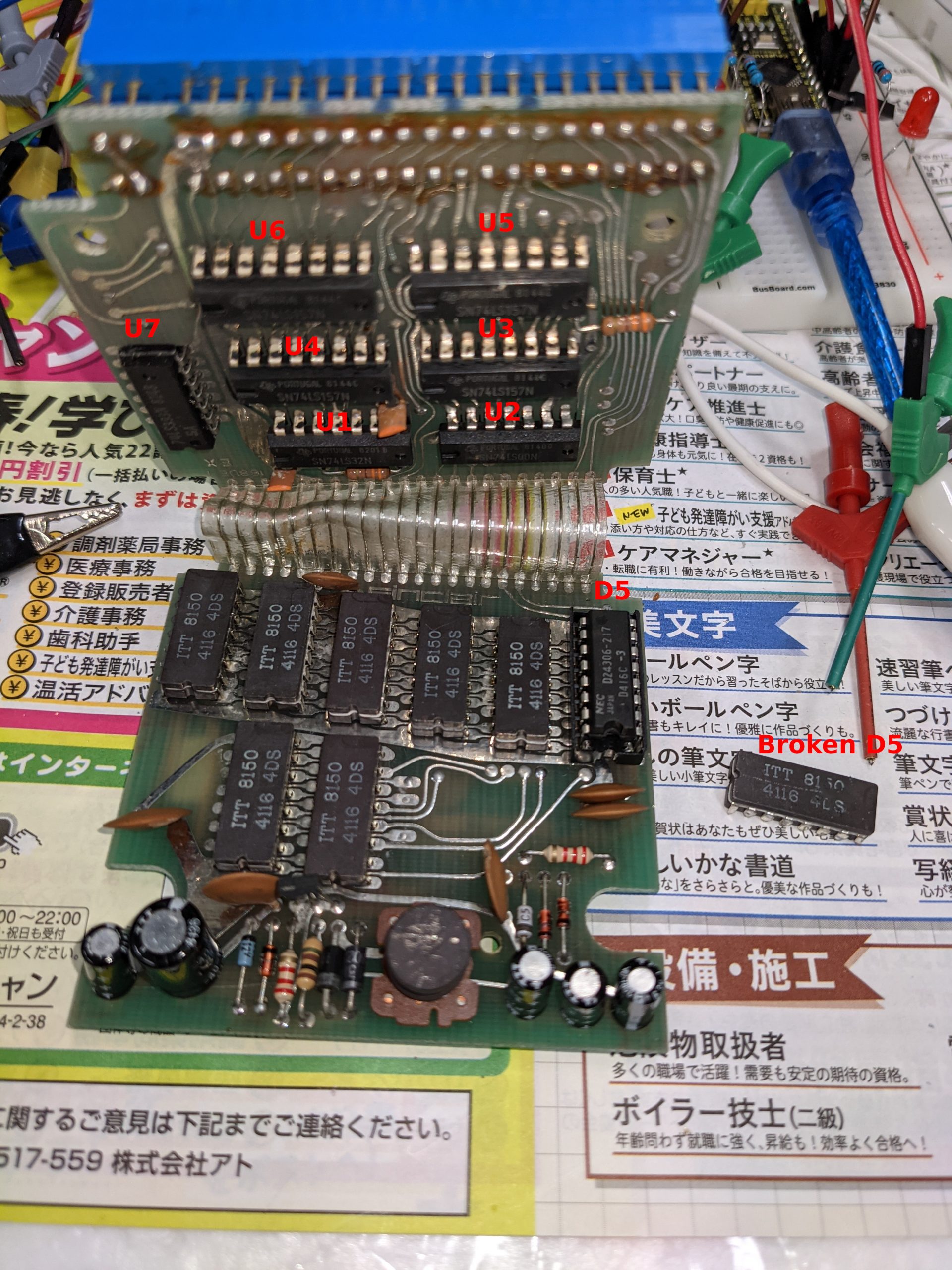
The ZX81 RAM pack is made of two circuit boards. These circuit boards are sandwiched together. The pins connecting the two boards are very flexible, so you can just apply a small amount of force and bend the two boards apart. One board has logic chips (the aforementioned NAND chip, an OR chip, four data selector chips (74LS157) and a dual 4-bit counter chip (74LS393)). The other has the DRAM chips and some circuitry to generate -5V and 12V from 5V and 9V input. My voltages were all good and I didn’t see anything unusual there, so I didn’t really look into it too much. If you need to debug the power circuitry, you may need to know how to generate negative voltage (https://www.allaboutcircuits.com/projects/build-your-own-negative-voltage-generator/). I also created a rough simulation of the power circuitry on https://www.falstad.com/circuit/. If you are interested, go to File -> Import from Text and paste the following code, but I don’t think I’m using the correct transformer and there may be other issues:
$ 1 0.000005 24.46919322642204 50 5 43 5e-11
169 112 112 192 112 0 4 9 -1.3552527156068805e-20 0.05437017461335131 0.022386130031495474 0.99
R 192 112 128 64 0 0 40 9 0 0 0.5
w 192 144 272 144 0
w 272 144 272 256 0
t 240 272 272 272 0 -1 17.389821061615624 -0.6849346284276479 100 default
w 272 288 272 336 0
w 192 224 288 224 0
d 336 224 288 224 2 default
34 zener-12 1 1.7143528192810002e-7 0 2.0000000000000084 12 1
z 336 224 400 224 2 zener-12
d 336 224 336 256 2 default
w 336 256 336 336 0
r 192 224 192 272 0 100
w 192 272 240 272 0
r 192 272 192 336 0 2200
g 192 336 144 336 0 0
w 192 336 272 336 0
w 304 336 336 336 0
w 192 176 224 176 0
w 224 176 224 384 0
w 272 336 304 336 0
d 304 384 304 336 2 default
d 352 384 304 384 2 default
r 352 384 416 384 0 2200
34 zener-5.1 1 1.7143528192810002e-7 0 2.0000000000000084 5.1 1
z 416 384 416 336 2 zener-5.1
209 352 336 352 384 0 0.000001 5.679241726295006 1 1
w 224 176 352 176 0
d 352 176 400 176 2 default
w 400 176 400 224 0
d 400 112 400 176 2 default
w 192 112 400 112 0
w 400 112 464 112 0
w 416 384 448 384 0
w 416 336 464 336 0
w 464 336 464 256 0
209 464 208 464 256 0 0.000022000000000000003 8.999999999994335 1 1
w 464 112 464 160 0
c 400 224 400 336 0 0.00009999999999999999 9.397384509781268 0.001
w 352 336 400 336 0
w 336 336 352 336 0
w 400 336 416 336 0
O 384 416 432 416 1 0
O 400 224 448 224 1 0
c 192 176 192 224 0 0.000022 -18.406729087662764 0.001
c 224 384 304 384 0 0.000001 -0.8460828370149334 0.001
r 464 160 464 208 0 1000
r 448 384 512 384 0 1000000
g 512 384 560 384 0 0
x 9 10 431 32 4 16 ZX81\sRAM\spack\spower\ssupply\scircuit\s(9V\s->\s-5,\s12V).\\nChanged\ssome\scapacitors\sto\snon-polarized
x 489 171 629 212 4 16 Added\s1k\sresistor\\nto\sprevent\sshort\\ncircuit
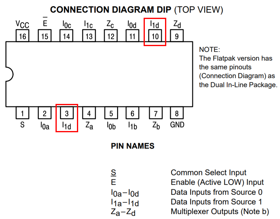
The four 74LS157 selector chips on the non-DRAM board work as two separate entities, that is, the “selector” inputs are tied together for the lower two chips and tied together for the higher two chips. When you look for 74LS157 pinouts on the internet, you’ll often find an OCR’d and slightly wrong pinout. The pin labelled I1d on the bottom side should be labelled I1a instead:
The 74LS393 is used by the ZX81 to refresh the DRAM. According to the datasheet, the DRAM has to be refreshed at least every 2 ms. I am guessing that the CPU or ULA periodically generates the RFSH signal, but we don’t have to worry about that in the context of this repair. Each time RFSH goes low (low because there is a NOT gate built from one of the NAND gates between RFSH and pin 1 (“clock”) of the 74LS393 counter chip), the counter chip adds +1 to its internal state. Additionally, the RFSH signal also goes into the first pair of selector chips, which causes the output of the counter to be selected as the output. Otherwise, address lines A0-A6 are used as the output.
The second pair of selector chips has address lines A7-A13 as one set of inputs, and the output of the previous selector chip as the other set of inputs. The circuit that goes into the selector pin is somewhat complicated, as it uses four different inputs to decide which set of inputs to select. I decided to make a truth table to better understand it. If you need to understand this circuit, the truth table or OpenDocument / Excel files below may help a little bit:
| Write operation: | ||||||||
| WR | MREQ | RD | temp1 nand(wr,rd) | A14 | temp2 nand(temp1,A14) | S or(mreq,temp2) | ||
| 0 | 0 | 0 | 1 | 0 | 1 | 1 | 1 | |
| 0 | 0 | 0 | 1 | 1 | 0 | 0 | 2 | |
| 0 | 0 | 1 | 1 | 0 | 1 | 1 | 3 | |
| 0 | 0 | 1 | 1 | 1 | 0 | 0 | 4 | |
| 0 | 1 | 0 | 1 | 0 | 1 | 1 | 5 | |
| 0 | 1 | 0 | 1 | 1 | 0 | 1 | 6 | |
| 0 | 1 | 1 | 1 | 0 | 1 | 1 | 7 | |
| 0 | 1 | 1 | 1 | 1 | 0 | 1 | 8 | |
| Read operation: | ||||||||
| WR | MREQ | RD | temp1 nand(wr,rd) | A14 | temp2 nand(temp1,A14) | S or(mreq,temp2) | ||
| 1 | 0 | 0 | 1 | 0 | 1 | 1 | 9 | |
| 1 | 0 | 0 | 1 | 1 | 0 | 0 | 10 | |
| 1 | 0 | 1 | 0 | 0 | 1 | 1 | 11 | |
| 1 | 0 | 1 | 0 | 1 | 1 | 1 | 12 | |
| 1 | 1 | 0 | 1 | 0 | 1 | 1 | 13 | |
| 1 | 1 | 0 | 1 | 1 | 0 | 1 | 14 | |
| 1 | 1 | 1 | 0 | 0 | 1 | 1 | 15 | |
| 1 | 1 | 1 | 0 | 1 | 1 | 1 | 16 |
The circuit contains a number of RC delay circuits to make the timing work, but as the delay is on the order of 10-20 ns, I don’t have to worry about those when driving this circuit using an Arduino — I’m using digitalRead() and digitalWrite(), and these functions take a couple of microseconds to complete. Looking at the timing diagram in the DRAM IC’s datasheet however, it is relatively obvious that these delays are needed.
As stated above, the DRAMs are all connected in parallel on all pins except the data pins. And while the DRAM chips have separate pins for input and output, the RAM pack ties these together as they are of course not used at the same time — you either read or write.
Some more notes on the timing — programming the Arduino like this will drive the chips very slowly, but according to the datasheet, we don’t really have to worry about being too slow in most cases. Some parameters have “max” values on the order of 10s or 100s of ns, but the notes alleviate most concerns in that area. The maximum RAS/CAS pulse width of 32000/10000 ns should be okay with just digitalRead()/digitalWrite() (I didn’t measure too much though, to be honest). Here is the code doing the write and CAS pulses, and what we know about digitalWrite(), this should be just under 10000 ns:
void writeAddress(...) {
...
  /* write */
  digitalWrite(WR, LOW);

  /* tRCD max is 50 ns, but footnote 10 states:
   * "If tRCD is greater than the maximum recommended value shown in this table, tRAC will increase by the amount that tRCD exceeds the value shown."
   * Therefore this is not a hard maximum and we don't have to worry too much about being too slow */
  digitalWrite(XA14, HIGH); /* pulls CAS low after 10-20ns */

  digitalWrite(WR, HIGH);
  digitalWrite(XA14, LOW);
Here’s an oscilloscope screenshot for just the WR pulse (which should have the same timing), which is approximately… 10 microseconds!

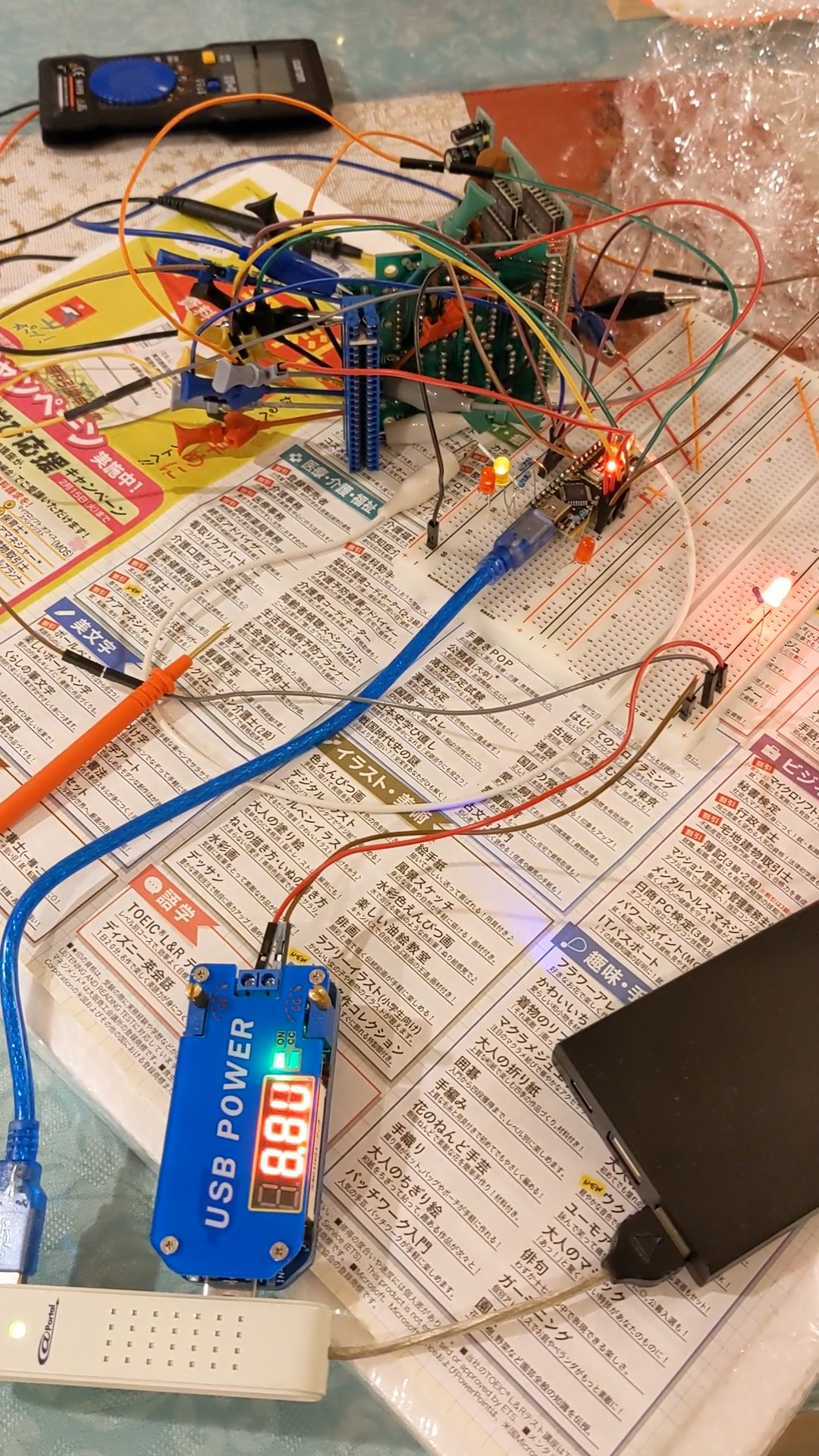
There is code out there to test 4116 RAM ICs. However, the chips in my RAM pack weren’t socketed so I couldn’t take them out very easily. And it’s not certain if we can just attach the Arduino directly to the DRAM chips’ pins — if we apply power to the board we will power up the rest of the circuitry and that could interfere with our testing — the selector chips might produce 1s when we want 0s, or vice versa. I took this code and modified it to work with the rest of the circuitry. I originally planned on testing two bits at once (i.e., two DRAM chips at once), but I ran out of cables. I’ve left in the code however, commented.
Since we don’t have a lot of pins on the Arduino (or connectors that we can use to connect the Arduino with the RAM pack), I decided to enlist the binary counter chip’s help to generate the addresses. Check out the advanceRow() function to see how easy this is — we just need to manipulate RFSH. (Note that “row” means the same thing as it does in the datasheet — the DRAM chip is organized into 128 “rows” and 128 “columns”, 128×128 = 16384 bits.)
I also decided to write two different values in two successive addresses before reading back from these addresses. This is important because otherwise the Arduino may just read whatever it just put on the wire itself. I.e., if you take an Arduino that isn’t connected to anything at all and do something like the following, your digitalRead may return whatever you wrote using digitalWrite!
digitalWrite(13, HIGH);
val = digitalRead(13); // val may be 1 now!
Which is why we instead do something like this (c is column, v is value, row is set elsewhere):
        writeAddress(c, v, v);
        writeAddress(c+1, !v, !v);
        readAddress(c, &read_v0_0, &read_v1_0);
        readAddress(c+1, &read_v0_1, &read_v1_1);
I also changed the error() and ok() functions. ok() will make a (preferably green) LED blink slowly, error() will made a (preferably red) LED and the other LED blink alternatingly.
Here is the code:
/* Modified by sneep to test the Sinclair ZX81 RAM pack.
* Original code is at http://labs.frostbox.net/2020/03/24/4116-d-ram-tester-with-schematics-and-code/
* The Arduino doesn't have enough pins to check all outputs at
* the same time so we'll test one (out of eight) at a time;
* rewiring is required between tests.
*
* Unlike the previous version of this source code, we go through
* the onboard logic (a couple of ORs, ANDs, multiplexers, and a
* counter for refresh) rather than talking to the 4116 RAM ICs
* directly.
* It's probably not possible to check the 4116 chips in-circuit
* using the original source code, as we would apply power to
* everything and would then cause our address signals to fight
* against the multiplexer's outputs.
*
* NOTE: As we are using digitalWrite, this is a very slow test.
* We go beyond the 'max' value recommended in the datasheet for
* one thing, and go way beyond the 'min' values -- borderline
* chips could pass our tests but fail when driven by the ZX81.
*
* NOTE: At least the init refresh cycles may stop working if we
* replace digitalWrite by something faster (init refresh).
*/
//This is for an arduino nano to test 4116 ram ic. Please see video https://youtu.be/MVZYB54VD2g and blogpost
//Cerated in november 2017. Code commented and posted march 2020.
//Most of the code and design is from http://forum.defence-force.org/viewtopic.php?p=15035&sid=17bf402b9c2fd97c8779668b8dde2044
//by forum member "iss"" and modified to work with 4116 D ram by me Uffe Lund-Hansen, Frostbox Labs.
//This is version 2 of the code. Version 1 had a very seroisl bug at approx. line 43 which meant it only checked ram address 0
//#include <SoftwareSerial.h>
#define XD0 A1
#define MREQ 5
#define WR 6
#define RFSH 10
#define XA7 4
#define XA8 2
#define XA9 3
#define XA10 A3 // orange
#define XA11 A4 // yellow
#define XA12 A5 // green
#define XA13 A2
#define XA14 A0
#define R_LED 13 // Arduino Nano on-board LED
#define G_LED 8
//Use the reset button to start the test on solder an external momentary button between RST pin and GND pin on arduino.
#define BUS_SIZE 7
#define NO_DEBUG 0
#define VERBOSE_1 1
#define VERBOSE_2 2
#define VERBOSE_3 3
#define VERBOSE_4 4
#define VERBOSE_MAX 5
#define DEBUG NO_DEBUG // VERBOSE_3
#define DEBUG_LED_DELAY 0 /* Set to 0 for normal operation. Adds a delay inbetween when double-toggling fast signals, e.g. RFSH */
int g_row = 0;
const unsigned int a_bus[BUS_SIZE] = {
XA7, XA8, XA9, XA10, XA11, XA12, XA13
};
void setBus(unsigned int a) {
int i;
/* Write lowest bit into lowest address line first, then next-lowest bit, etc. */
for (i = 0; i < BUS_SIZE; i++) {
digitalWrite(a_bus[i], a & 1);
a /= 2;
}
}
void advanceRow() {
/* Keep track of which row we're on so we can put that in our debug output */
g_row = (g_row + 1) % (1<<BUS_SIZE);
/* Counter chip should be fast enough.
* NOTE there is a NOT gate between arduino pin and counter chip */
digitalWrite(RFSH, LOW);
if (DEBUG_LED_DELAY) {
interrupts();
delay(DEBUG_LED_DELAY);
noInterrupts();
}
digitalWrite(RFSH, HIGH);
}
void writeAddress(unsigned int c, int v0, int v1) {
/* Set column address in advance (arduino may be too slow to set this later) (won't appear on the RAM chip pins yet) */
setBus(c);
if (DEBUG >= VERBOSE_MAX) {
interrupts();
Serial.print("Writing v0 ");
Serial.println(v0);
// Serial.print("Writing v1 ");
// Serial.println(v1);
noInterrupts();
}
/* Set val in advance (arduino may be too slow to set this later) (chip doesn't care what's on this pin except when it's looking) */
pinMode(XD0, OUTPUT);
// pinMode(XD1, OUTPUT);
digitalWrite(XD0, (v0 & 1)? HIGH : LOW);
// digitalWrite(XD1, (v1 & 1)? HIGH : LOW);
digitalWrite(MREQ, LOW); /* pulls RAS low */
/* write */
digitalWrite(WR, LOW);
/* tRCD max is 50 ns, but footnote 10 states:
* "If tRCD is greater than the maximum recommended value shown in this table, tRAC will increase by the amount that tRCD exceeds the value shown."
* Therefore this is not a hard maximum and we don't have to worry too much about being too slow */
digitalWrite(XA14, HIGH); /* pulls CAS low after 10-20ns */
digitalWrite(WR, HIGH);
digitalWrite(XA14, LOW);
digitalWrite(MREQ, HIGH);
pinMode(XD0, INPUT);
// pinMode(XD1, INPUT);
}
void readAddress(unsigned int c, int *ret0, int *ret1) {
/* set column address (won't appear on the RAM chip pins yet) */
setBus(c);
digitalWrite(MREQ, LOW); /* pulls RAS low, row address will be read in after tRAH (20-25 ns) */
/* Need to wait tRCD (RAS to CAS delay time), min. 20ns max. 50 ns, but a footnote implies that we can go over the max */
digitalWrite(XA14, HIGH); /* sets S to high and pulls CAS low after 10-20ns (it's correct to have the column address on the bus before pulling CAS low) */
/* Need to wait tCAC (time CAS-low to data-valid), but Arduino is slow enough for our purposes */
/* get current value
* datasheet "DATA OUTPUT CONTROL", p. 8:
* "Once having gone active, the output will remain valid until CAS is taken to the precharge (logic 1) state, whether or not RAS goes into precharge."
*/
*ret0 = digitalRead(XD0);
// *ret1 = digitalRead(XD1);
digitalWrite(XA14, LOW);
digitalWrite(MREQ, HIGH);
}
void error(int c, int v, int read_v0_0, int read_v1_0, int read_v0_1, int read_v1_1)
{
unsigned long a = ((unsigned long)c << BUS_SIZE) + g_row;
interrupts();
Serial.print(" FAILED $");
Serial.println(a, HEX);
Serial.print("Wrote v/!v: ");
Serial.println(v);
Serial.println(!v);
Serial.print("Read v0_0: ");
Serial.println(read_v0_0);
// Serial.print("Read v1_0: ");
// Serial.println(read_v1_0);
Serial.print("Read v0_1: ");
Serial.println(read_v0_1);
// Serial.print("Read v1_1: ");
// Serial.println(read_v1_1);
Serial.flush();
while (1) {
blink_abekobe(100);
}
}
void ok(void)
{
digitalWrite(R_LED, LOW);
digitalWrite(G_LED, LOW);
interrupts();
Serial.println(" OK!");
Serial.flush();
while (1) {
blink_green(500);
}
}
void blink_abekobe(int interval)
{
digitalWrite(R_LED, LOW);
digitalWrite(G_LED, HIGH);
delay(interval);
digitalWrite(R_LED, HIGH);
digitalWrite(G_LED, LOW);
delay(interval);
}
void blink_green(int interval)
{
digitalWrite(G_LED, HIGH);
delay(interval);
digitalWrite(G_LED, LOW);
delay(interval);
}
void blink_redgreen(int interval)
{
digitalWrite(R_LED, HIGH);
digitalWrite(G_LED, HIGH);
delay(interval);
digitalWrite(R_LED, LOW);
digitalWrite(G_LED, LOW);
delay(interval);
}
void green(int v) {
digitalWrite(G_LED, v);
}
void fill(int v) {
int i, r, c, g = 0;
int read_v0_0, read_v1_0;
int read_v0_1, read_v1_1;
if (DEBUG >= VERBOSE_1) {
Serial.print("Writing v: ");
Serial.println(v);
}
for (r = 0; r < (1<<BUS_SIZE); r++) {
if (DEBUG >= VERBOSE_1) {
interrupts();
Serial.print("Writing to row ");
Serial.println(g_row);
noInterrupts();
}
for (c = 0; c < (1<<BUS_SIZE); c++) {
if (DEBUG >= VERBOSE_4) {
interrupts();
Serial.print("Writing to column ");
Serial.println(c);
noInterrupts();
}
green(g ? HIGH : LOW);
/* The same two data pins are used for both read and write,
* so when nothing is connected we would just read the value we just wrote.
* So let's write 0 and 1 (or 1 and 0) to two addresses and read them back.
* We should get 0 and 1, but if there's nothing connected we'd get 1 and 0,
* which
*/
writeAddress(c, v, v);
writeAddress(c+1, !v, !v);
readAddress(c, &read_v0_0, &read_v1_0);
readAddress(c+1, &read_v0_1, &read_v1_1);
if (DEBUG >= VERBOSE_3) {
interrupts();
Serial.print("Read v0_0: ");
Serial.println(read_v0_0);
// Serial.print("Read v1_0: ");
// Serial.println(read_v1_0);
Serial.print("Read v0_1: ");
Serial.println(read_v0_1);
// Serial.print("Read v1_1: ");
// Serial.println(read_v1_1);
noInterrupts();
}
if ((read_v0_0 != v) || // (read_v1_0 != v) ||
(read_v0_1 != !v)) { //|| (read_v1_1 != v)) {
error(c, v,
read_v0_0,
read_v1_0,
read_v0_1,
read_v1_1);
}
g ^= 1;
}
advanceRow();
}
for (i = 0; i < 50; i++) {
blink_redgreen(100);
}
}
void setup() {
int i;
Serial.begin(115200);
while (!Serial)
; /* wait */
Serial.println();
Serial.print("ZX81 RAM PACK TESTER");
for (i = 0; i < BUS_SIZE; i++)
pinMode(a_bus[i], OUTPUT);
pinMode(XA14, OUTPUT);
pinMode(MREQ, OUTPUT);
pinMode(WR, OUTPUT);
pinMode(R_LED, OUTPUT);
pinMode(G_LED, OUTPUT);
/* Input and output is tied together on RAM pack.
* We'll leave the pinMode on INPUT for most of the time and only set to OUTPUT when writing.
*/
pinMode(XD0, INPUT);
// pinMode(XD1, INPUT);
digitalWrite(WR, HIGH);
digitalWrite(MREQ, HIGH);
digitalWrite(XA14, HIGH);
Serial.flush();
digitalWrite(R_LED, LOW);
digitalWrite(G_LED, LOW);
noInterrupts();
/* Datasheet says: "Several cycles are required after power-up before proper device operation is achieved. Any 8 cycles which perform refresh are adequate for this purpose."
* We'll just perform a refresh on all rows. */
for (i = 0; i < (1<<BUS_SIZE); i++) {
/* Should work fine timing-wise with standard Arduino digitalWrite() (tRC min: 375 ns, no max apparently) */
interrupts();
Serial.print("init: refreshing row ");
Serial.println(g_row);
Serial.flush();
noInterrupts();
advanceRow();
digitalWrite(MREQ, LOW);
digitalWrite(MREQ, HIGH);
}
}
void loop() {
interrupts(); Serial.print("."); Serial.flush(); noInterrupts(); fill(0);
interrupts(); Serial.print("."); Serial.flush(); noInterrupts(); fill(1);
ok();
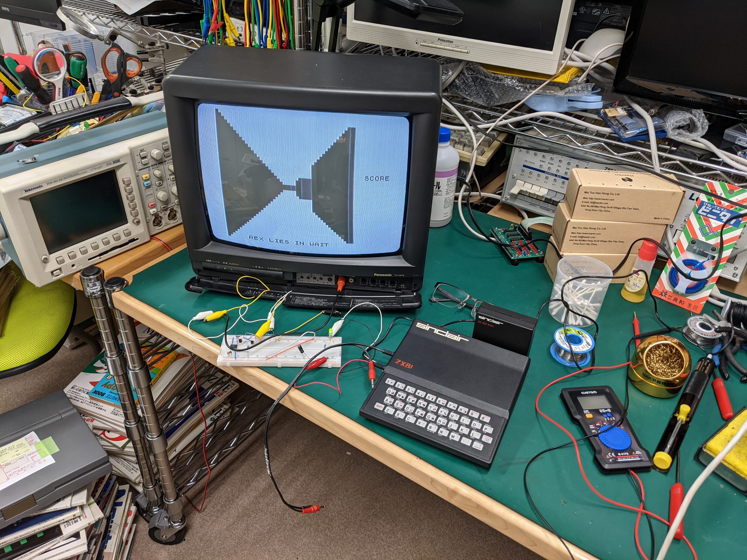
}In my case, all DRAM chips passed the test except the one controlling D5. Even the very first read wouldn’t work out. I therefore replaced that one and hooray, things worked again! Here’s a pic of a 3d maze game running with the repaired RAM.
Some random notes on how to do the actual replacement
Before replacing the defective RAM chip I also tried piggybacking, but that didn’t make the test pass. I was planning on using my oscilloscope to get an idea of what’s going wrong when piggybacking, but things were just too finicky and I abandoned that plan. If you try yourself, make sure to put your multimeter in continuity mode and check that your piggybacked RAM chip is actually making contact.
I cut off the legs of the chip I 99% knew was bad and then desoldered the legs. Applying heat using a soldering iron from above and using a desoldering pump from below (or the other way round) worked reasonably well.
It should be okay to use a socket on most chips. Here’s a photo of the boards sandwiched up again after the replacement. You can see that there’s quite some clearance left:

Let me know if you have any questions about this repair.