Hi! My sabbatical ended and I’ve been working again since two months ago. Boo. However there’s this thing I just wanted to get off my chest, so I spent a few hours that I did not really have and wrote some code and this blog post about it!
Last year, I made a 4164/4116 DRAM tester for the Raspberry Pi Pico, which works just as you would expect, you program the Pico, place it on a breadboard, add some wires and something to drop the 5V to 3.3V for the Q output, place the 4164 or 4116 chip you’d like to test on the breadboard, connect a USB cable from the Pico to a computer, and look at the terminal output (or just the on-board LED). This is useful if you have already extracted a 4164 chip that you have determined to be bad. (I have written previously how you could determine whether a 4164 chip is bad, here and here.)
I previously made a “live” chip tester for the Arduino, capable of checking whether simple logic chips are doing what they’re supposed to be doing in a powered on system. I used the Arduino rather than the Pico because the Arduino is 5V tolerant. In this post, we’re not doing simple logic chips, but DRAM chips. And since we need to be super-fast, we’re using a Pico.
Executive summary
We “allocate” 64 KB of RAM on the Pico. We need to read in two 8-bit addresses, and combine them to a 16-bit address. If a write is being attempted, we write the same bit value into the appropriate address of Pico’s RAM. If a read is being attempted, we check if the DRAM’s output is the same as what we have in the Pico’s RAM. (We could also use 64 Kb of RAM on the Pico at a minimum, but as we’ll see in the next section we do not really have a lot of time for such shenanigans.)
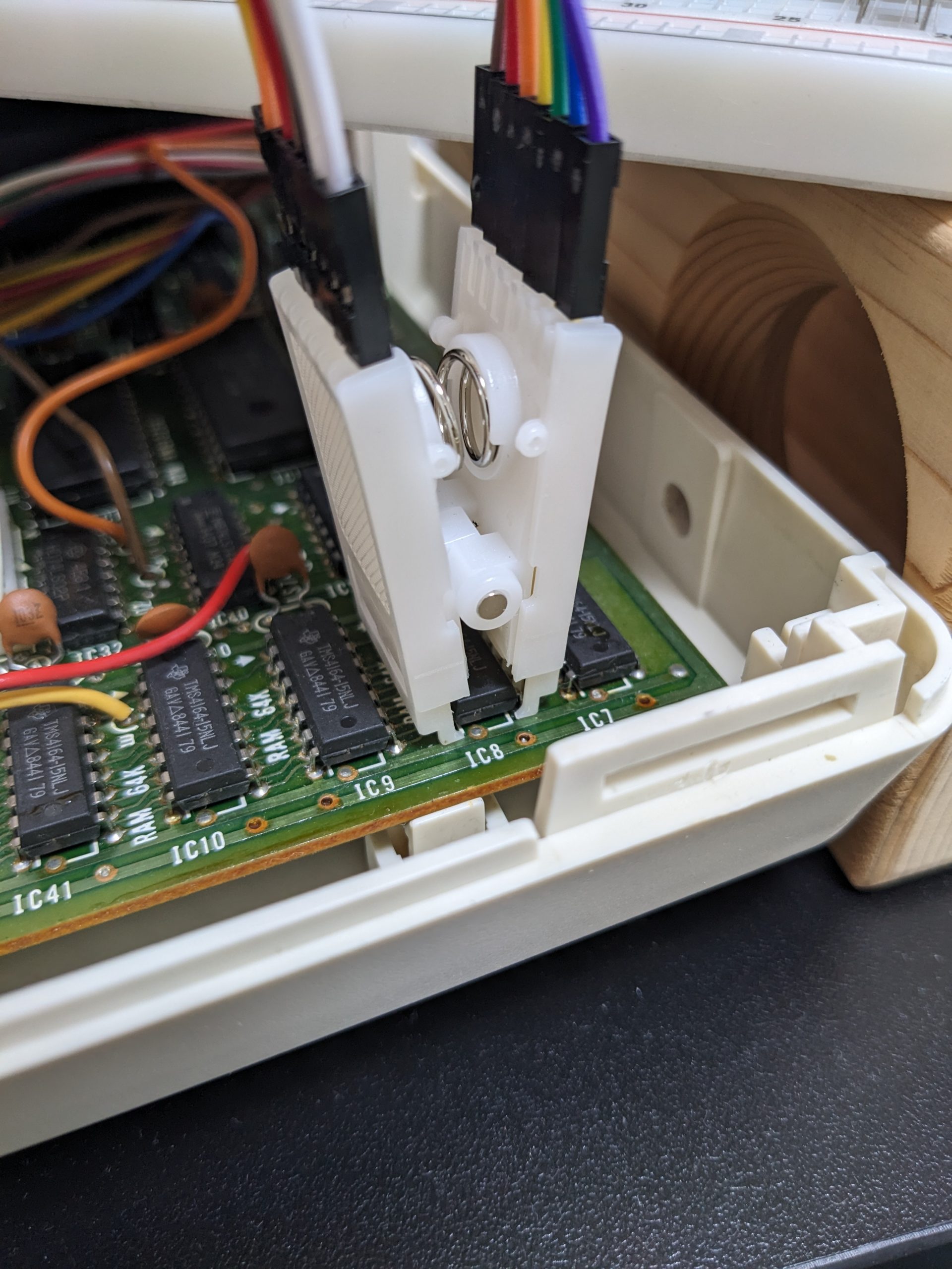
To use this software, having an IC test clip would probably be very beneficial. I use these: https://www.kandh.com.tw/ic-test-clips-ic-test-clips.html. These are available in Akihabara from Akizuki: https://akizukidenshi.com/catalog/g/gC-04753/. If they aren’t available in your market, perhaps these somewhat expensive test clips from 3M might be more available: https://www.digikey.jp/ja/products/detail/3m/923700/3852.
Note: to use this software, you need to at least mostly know what you’re doing.
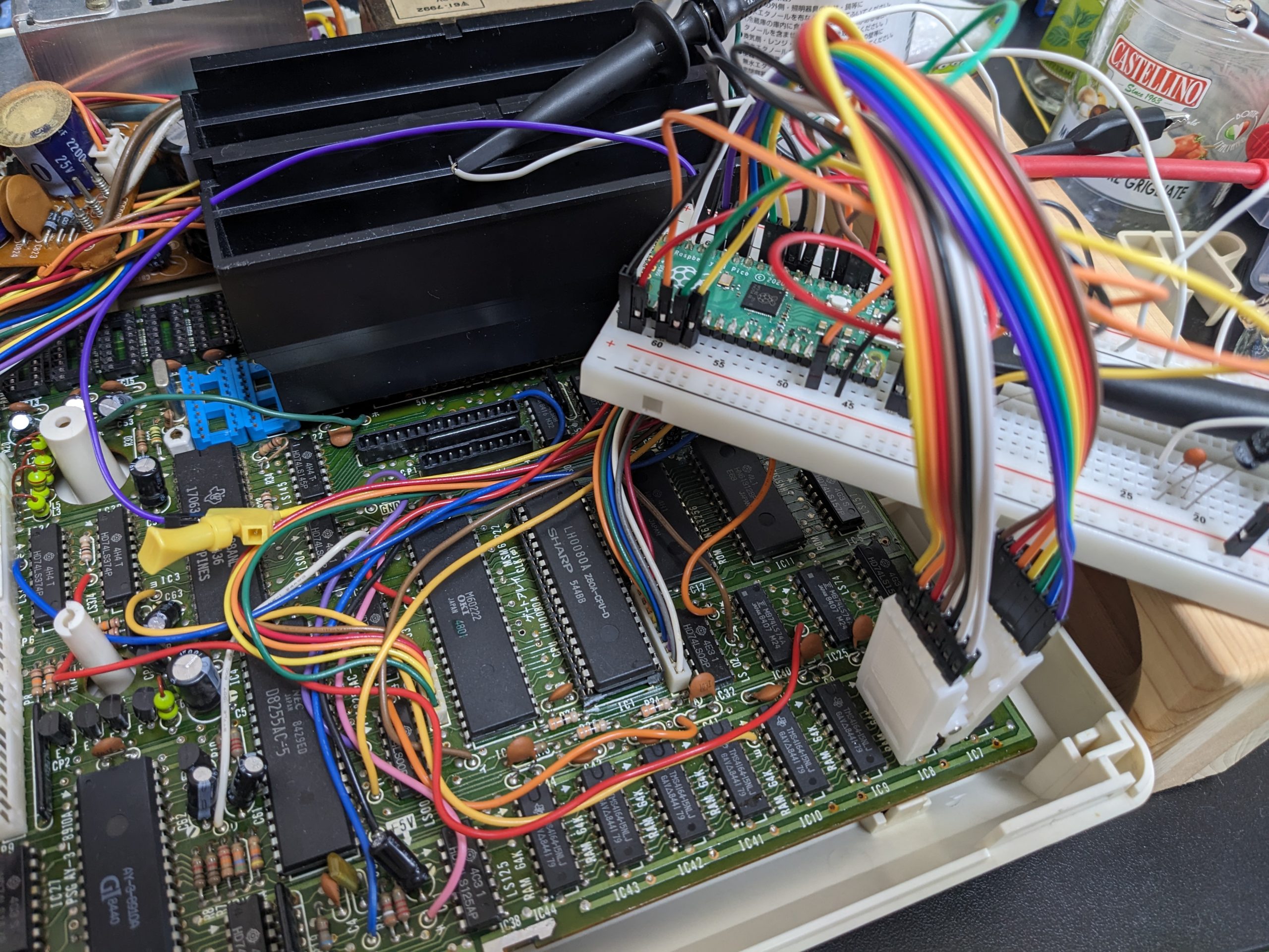
One note on hooking up the Pico directly to 5V components, as seen in the above pictures
Not guaranteed to not fry your Pico (note the double negation), do this at your own risk. Your Pico will possibly also draw more current than a normal TTL chip when driven above 3.6V or so, which could easily damage your precious hardware! (The current on the address pins will likely be supplied by a pair of 74LS157 chips, on the Q pins by the RAM chip, and the current on the RAM’s data in pin by the CPU or any other. \RAS and \CAS probably by custom logic chips.) Use a 74HCT245 between the Pico and the device you’d like to test.
Caveat 1
The Pico is very fast when compared to an 8-bit computer from the 1980s, but 4164 transition times are extremely fast too. If you look at a timing diagram for the 4164 (which you will find in any 4164 datasheet), you will notice that all transition times listed are on the order of <ten, tens, or low hundreds of nanoseconds. Most 4164 chips have a -20, -15, -12, or -10 suffix in their part number. This indicates the minimum allowable number of nanoseconds × 10 for the sum of all transitions. (If the DRAM is driven faster, it probably won’t work correctly. However, if it’s driven slower, most things will generally work out, though if your system e.g. reads the DRAM’s output too slowly it might be too late and not work out.)
The stock Pico runs at 125 MHz, which means that one CPU cycle is 8 ns. From hearsay, you can probably overclock any Pico to 200 MHz (clock cycles are 5 ns), and many people report that their Pico runs fine even at 400 MHz (clock cycles are 2.5 ns). For -15 DRAMs, you have 150/8 = 18.75 CPU cycles per transition if the DRAM is driven at its max speed. (Note: it isn’t on MSX machines, at least.) 18 CPU cycles isn’t a lot. Remember, we need to convert two 8-bit addresses to a 16-bit address, and then check if the newly read value matches our previously recorded value. Is that doable in 18 CPU cycles? I don’t think so, but I’m not an ARM assembly expert.
So, did I get it to work? Well… sort of but not quite.
Caveat 2
Note that there are many failure modes for DRAM chips. For example, if the chip gets super-hot within a few seconds, it’s probably shorted. I’d expect there to be a very low resistance between ground and another pin. Before hooking up the “live” tester I’m going to explain on this page, check for that kind of stuff. I would not recommend using the live tester on a chip that gets super-hot within seconds. You could risk melting your connectors, and if the short is not between VCC and GND, potentially also risk your Pico due to excessive current on a pin driven by the Pico.
Caveat 3
Untested with 4116 chips, only tested with my MSX’s main RAM.
Current status
The live tester successfully verifies that a TMS4164-15 DRAM chip under test in my stand-alone 4164 RAM tester is outputting the correct values. (There is no reason why it shouldn’t work with a 4116 chip. The tester certainly does! You just need to re-wire slightly. Also, 5V on the Pico, yeah, it doesn’t seem to “explode immediately.” But -5V or 12V? You’d better leave those pins unconnected!)
On a real system (my trusty Hitachi MB-H2 MSX) with TMS4164-15NL DRAM chips, the live tester manages just fine from power up, up until the first ~11000 comparisons (which is a split second), but at some point reads a 0 when it should have been a 1, and prints an error. Printing errors takes a long time at 115200 bps, so we go completely off the rails once we’ve encountered the first error. (That’s slightly configurable though, see “Lnobs” section for details.)
However, in the live tester’s “DEBUG” mode, it just collects a lot of samples into memory, and prints them out when the sample memory is full. Using a simple script (the Perl script included in the repo), I can then verify that all the samples check out. Note that the DEBUG code also prints out who many times it had to wait until it got data from the PIO. The answer is 0 times every time, which means that we’re too slow or almost too slow. (Sometimes there is a handful of mismatches, I’ll look into those at some point. Could be that we were just too slow, or the 5V is messing with the system ;D)
There’s a lot that could be improved, hence the “WIP” attribute in title. The first obvious improvement would be to try a little harder in the non-debug mode. The Pico has two CPU cores, and we’re only using one. We could attain more throughput by running according to the following scheme:
Core 1:
Wait for sample 1
Tell core 2 to wait for sample 2
Process sample 1
Wait for sample 3
Tell core 2 to wait for sample 4
Process sample 3
…
Core 2:
Wait for instructions from CPU 1
Wait for sample 2
Process sample 2
Wait for instructions from CPU 1
Wait for sample 4
Process sample 2
…
Another potential optimization would be to write the processing code in ARM assembly. (My experience with ARM assembly is mostly read-only, so not sure how much better I can get without spending way too much effort.)
Also I haven’t tried overclocking yet. Probably should!
Some more technical details
We use two PIO state machines. One waits for RAS high→low (“RAS SM”, and the other one waits for CAS high→low (“CAS SM”, which comes after the RAS transition.
Not all RAS transitions are followed by CAS transitions. For example, refresh is mostly RAS-only. In addition, though perhaps not used on the MSX(?), RAS transitions may be followed by multiple CAS transitions.
In the C code, we wait for events on the CAS SM, and then read from both the RAS SM’s FIFO and the CAS SM’s FIFO. In the PIO code, the CAS SM tells the RAS SM whether to push its address or not. (We could alternatively (maybe) always push and have the CPU make sure the FIFO never gets full, but my experiments in that regard didn’t go that well.)
There are a lot of defines that change the way the system works.
Knobs
- Setting PRINT_ERROR_THRESHOLD to something above 0 only starts printing errors after encountering that many errors.
- CORRECT_ERRORS causes the Pico’s memory to be updated when we encounter a mismatch
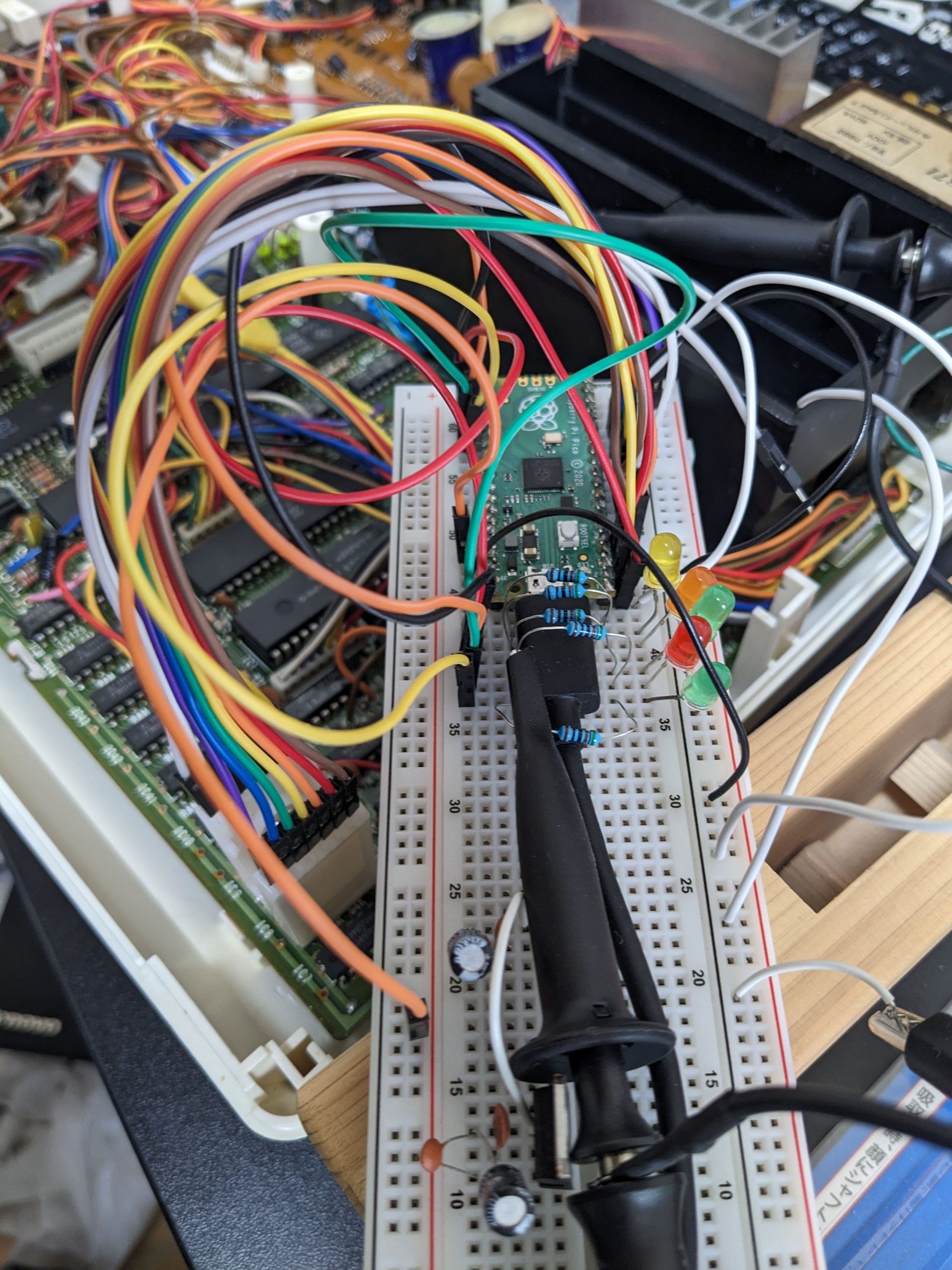
- VERBOSE_STATUS_LEDS causes the Pico to perform GPIO writes at GPIO16+ (or so, I recommend you check the source to find the exact GPIO pin number) to indicate whether we’re reading or writing. This isn’t very beneficial performance-wise.
- SWAP_RAS_AND_CAS_ADDRESSES: my Hitachi MB-H2 MSX applies the CPU’s A0-A7 to the RAM pins at RAS time, and A8-A15 at CAS time. When thinking “rows” and “columns”, most people would probably assume that “rows” use the more significant bits, but that is not necessarily the case, and it doesn’t matter. When operating in DEBUG mode, you’ll see accesses that are mostly linear if this define is set correctly. Otherwise each access will be 256 apart.
The code is at https://github.com/qiqitori/pico_live_chip_tester.
So… is this likely to find a fault?
I haven’t seen any DRAM chip failures (except on YouTube) where only some addresses were broken and the chip appeared to work otherwise. (SRAM chips are different story. I’m sort of planning on doing an SRAM tester too, but probably not too soon.) Most DRAM chips I’ve seen are an all-or-nothing affair. For all-or-nothing affairs, this chip tester is very likely to find the problem immediately, especially if you compare all 8 chips and only one is weird. For hypothetical chips with just a single address problem (or perhaps, a single broken row), either it’ll be difficult with the code not 100% working right now, or it might take several attempts and statistics.