Jump to ZX80 replica PCB Gerber files
A while ago, I watched a series of videos by DrMattRegan on the ZX80 and was very impressed with the uber-hacks the designers put in there. I’m not going to go into much detail here, but here is a set of facts that may pique your interest:
- The CPU’s A6 pin is permanently shorted to its \INT pin
- The ZX80 has only 1 KB of RAM
- The RAM is SRAM but the CPU’s internal DRAM refresh counter is not wasted
Additionally, the ZX81 was one of the first retro computers I ever repaired (article 1, article 2), which made the prospects of getting a ZX80 of my own even more attractive to me.
You have a lot of options if you want to build a ZX80 yourself. First of all, all the ICs (except the 2114 SRAM) can be bought new. There are multiple PCB designs that you can download for free, some electrically equivalent, some using chips that are a little more common than the ones on the original PCB. (For example, apart from the 2114 RAM, the 74LS93 is pretty rare because it is essentially useless nowadays. It was probably cheaper than the other 74-series counter ICs about 50 years ago, because a lot of “maybe nice to have” features were removed. It can easily be replaced using a different 74-series counter IC, and these days there really is no price difference.)
One thing that I really liked about the ZX81 that I worked on was the curved traces and the absence of solder mask on the traces. On this page by Grant Searle, you can find instructions to re-create the original PCB. There is a PDF that contains high-res images that look like this:
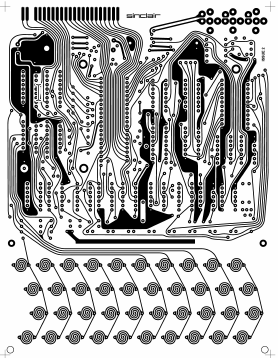
These can be printed out and turned into PCBs. I’m not much of a chemist, and even if the etching and tinning processes went well, I’d still need to do a bunch of drilling and then plate the newly drilled vias. Nowadays, there are companies such as PCBWay and JLCPCB that can do all this for you, and in an automated fashion, and for very attractive prices! (I do not intend to steer you away from etching PCBs yourself, in fact it always impresses me when people make PCBs themselves!)
However, these companies (currently?) do not accept bitmaps (as far as I know), they want Gerber files. So I traced the (600 dpi) bitmaps in Grant Searle’s PDF file and sent them out. I chose JLCPCB after some research because I found a pic of a board manufactured by JLCPCB that didn’t have any solder mask applied, and it looked pretty much the way I wanted it! However, I’m sure that PCBWay could do the same.
In order to get a board without solder mask, you have to get rid of the solder mask layer in the SVG or Gerber file, and you probably should also add a comment stating that this is intentional. I added this in my order, no guarantees the Chinese is correct: “The Gerber files don’t have a solder mask. This is intentional. Please do not apply a solder mask. Gerber文件没有焊膜。这是有意的。请不要应用焊膜。 我们有会说中文的人,所以如果你有什么问题,可以说中文。” I ordered 5 boards (which is the minimum order), lead-free HASL, white silkscreen (“ink-jet/screen printing silkscreen”), no gold fingers (not present on the original PCB either), regular PCB thickness (1.6 mm), regular outer copper weight (1 oz), regular via covering (tented), no castellated holes. JLCPCB’s customer service recommended I switch to ENIG, but it worked out fine with regular lead-free HASL. The price was $18.02 plus $11.70 shipping, minus the first time discount ($5).
When exporting the Gerber files in KiCad, you should follow the PCB manufacturer’s recommended settings. JLCPCB and probably most other places have a support page for this, this is JLCPCB’s.
Tracing bitmapped PCB foils
I used Inkscape to trace the PCBs in the PDF. Tracing is easy, you just load a bitmap and then go to “Path” -> “Trace Bitmap…”. But how do you convert that into Gerber files? Well, there is an extension that converts SVG files to KiCad files, svg2shenzhen.
It still took me many, many hours though. Why?
Converting traced holes to actual drill holes
svg2shenzhen expects “circle” shapes in a layer called “Drill”. If that layer doesn’t exist and/or it doesn’t contain circles, there won’t be any drill holes in your Gerber file. I wrote a very simple Inkscape extension to do this: Converting paths to circles in Inkscape
But first, we need to separate out the holes into a single layer. To do this, we first break apart the path containing all the traces (“Path” -> “Break Apart”). Then everything that isn’t connected together, and everything overlapping other things will exist as separate paths. Holes overlap other things and thus will be separate paths. And they will be obscured by the outer path. Now you just click on the surrounding path and remove it, perhaps like this:
One more consideration is hole size. Though the details are a little hazy now, selecting multiple circles and changing their size all at once didn’t work very well for me in Inkscape, so I just edited the SVG file directly.
The traced circles are paths that more or less look like circles, sure. But they’re often slightly oval or otherwise unshapely and not all the same size. So when you (after using the extension) crack open the SVG in a text editor, you may see that the radii are slightly different everywhere:
holes_circles.svg:    <circle
holes_circles.svg-       cx="50.392669494501675"
holes_circles.svg-       cy="193.60723742169256"
holes_circles.svg-       r="0.3154674216925315"
holes_circles.svg:       id="circle12107" />
holes_circles.svg:    <circle
holes_circles.svg-       cx="64.40136232421558"
holes_circles.svg-       cy="193.60780999999997"
holes_circles.svg-       r="0.31595000000000084"
holes_circles.svg:       id="circle12109" />
holes_circles.svg:    <circle
holes_circles.svg-       cx="78.4180010571009"
holes_circles.svg-       cy="193.60854169447143"
holes_circles.svg-       r="0.3165816944714095"
holes_circles.svg:       id="circle12111" />
I just did a find and replace operation here and used holes sizes that seemed good to me (after JLCPCB support telling me that my holes were rather small). And damn, by sheer dumb luck, I chose the best hole sizes ever (0.4 mm) and my jumper wires fit right into them without using clips; they make almost perfect contact. Maybe 0.375 mm or so would have been even better? (The other hole sizes I chose were 0.8 mm and 1 mm.) (Note: PCB manufacturers don’t have every drill bit in the universe, so 0.4 mm and 0.375 mm may just end up being the same drill bit.)
Update 2024-04-19: the holes for the headphone/microphone/power connectors are too tight though.
:(
Adhering to minimum spacing constraints
PCB manufacturers require that certain spacing constraints are observed. For example, traces may need to be 0.125 mm apart. The original bitmap you have may or may not adhere to the spacing constraints. I don’t know whether the bitmap in the PDF adheres to them! But I certainly do know that my order was rejected because the traces in my Gerber file weren’t quite up to snuff.
How would I even find out what my minimum spacing is? Well, I found this page by yet another company that makes PCBs: https://instantdfm.bayareacircuits.com/. This page analyzes your Gerber file and sends you a snazzy PDF with close-ups of your horrible transgressions. This is a screenshot from an early version of my Gerber files:
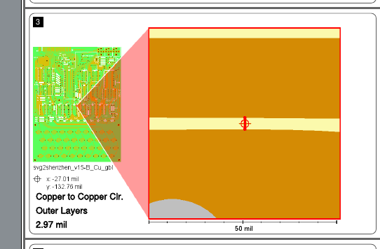
So I manually fixed this location and re-submitted, and sure enough, there were plenty of other similar narrow gaps. So I decided there must be a way to get Inkscape to find these critical regions, and this is what I came up with:
I just gave every object a 0.125/2 mm = 0.0625 mm border, and then zoomed in a bunch to look for objects that were touching each other. (Actually I probably added some to that value, but a couple months have passed and I don’t remember.)
Mistakes
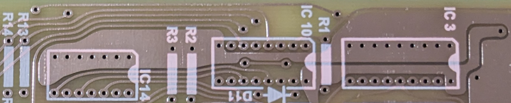
As mentioned earlier, in Inkscape, when you break apart a path that contains “holes”, you’ll end up with a large mass obscuring the holes. Here’s a video of exactly that:
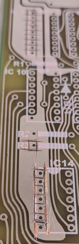
Well, I failed to notice that a number of holes within these black regions had been obscured. And thus they came out like this on the PCB:
While annoying, I was able to fix this using a utility knife. Boy, that utility knife’s blades went dull quick. (Luckily, my utility knife is one where you can just snap off consumed blade chunks. Having done this for the first time in my life, it was quite scary, to be honest. I did it behind a glass window.)
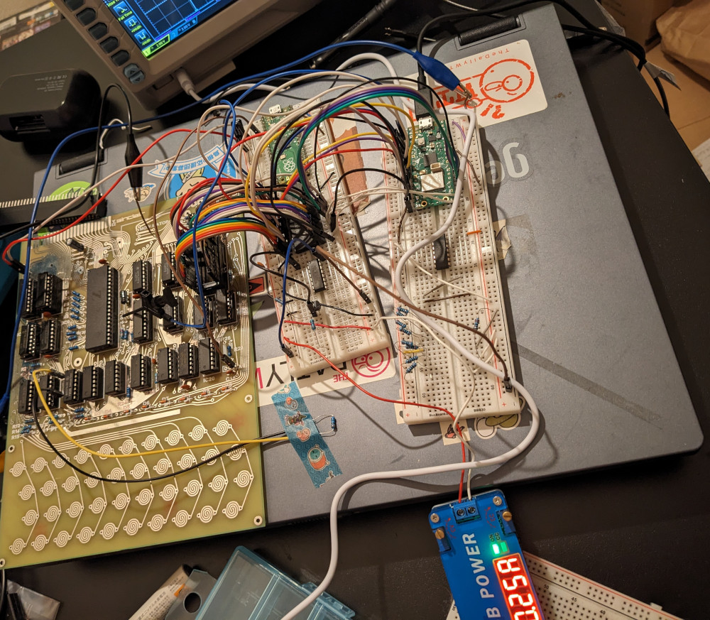
Procurement and assembly
After taking care of these mishaps, it was time to do a bunch of other stuff, such as celebrating Christmas and the New Year, and at some point bite the bullet and solder sockets and resistors and capacitors. I soldered everything using lead-free solder, and most or maybe even all of the components I put on the PCB are lead-free too, including the Z80! So maybe this is the first RoHS-compatible ZX81?! (Except the 2114 SRAM chips most likely aren’t RoHS-compatible. We’ll talk about those in a later section, BTW.)
I had half of the 74-series logic chips in stock. (From when I got Ben Eater’s DIY 8-bit computer, which I never assembled. I used the breadboards and some of the other components for a host of other things though!) The other half came from a small electronics shop right next to my office in Machida, サトー電気. I wanted a RoHS Z80 (print on chip ends in -PEG rather than -PEC), and bought it off Amazon.
Update 2024-04-19: Zilog/Littelfuse are reportedly discontinuing the original Z80 CPUs after almost 50 years of production! Maybe get them while they’re still available. Only source so far: https://www.mouser.com/PCN/Littelfuse_PCN_Z84C00.pdf (zilog.com still seems to list everything as “active” at the time of this writing)
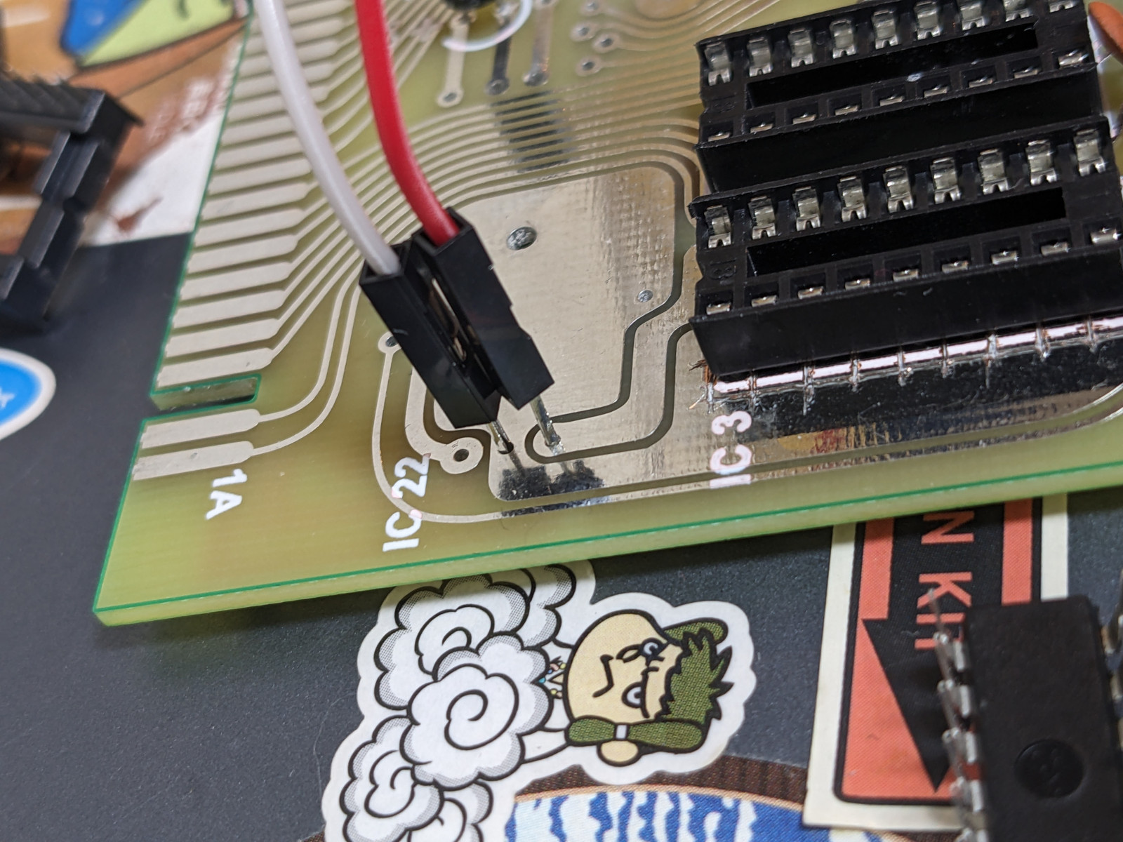
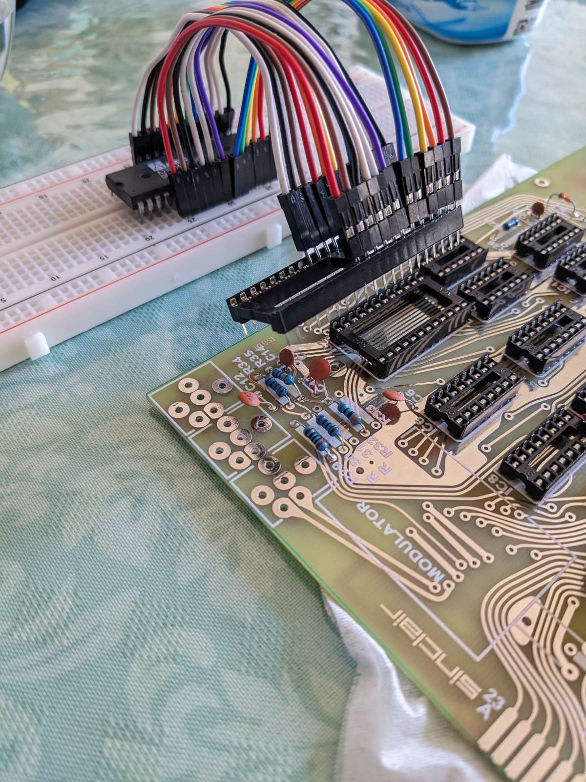
For the ROM I’m just using my EEPROM that I’ve been using in other projects. Since it’s huge and has a slightly different pinout, I’m currently using a breadboard as an adapter.
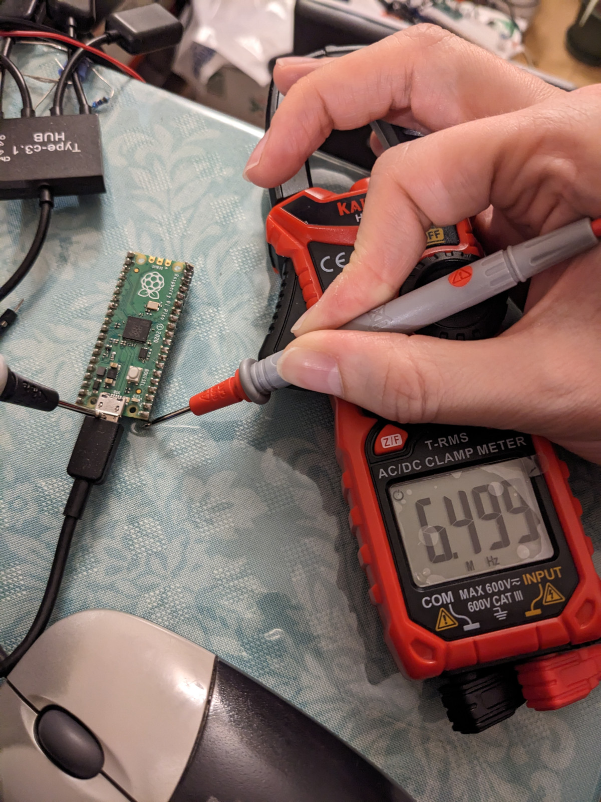
The only thing I couldn’t get anywhere, including Akihabara, is the 6.5 MHz oscillator. Many people use a 6.5536 MHz crystal in their ZX80 builds (hmm, I’ve seen a number like that before!) because the 6.5 MHz ones are pretty rare. But even those didn’t seem to exact in my neck of the woods. I ordered a 6.5 MHz oscillator off Digikey (through Marutsu) and will probably have it in a few days. (By the way, the original ZX80 used a 6.5 MHz ceramic resonator, but these seem to be just as unavailable. But who knows, maybe I could have gotten a 6 MHz one and filed it down a bit to get it to 6.5 MHz? But crystals work even better, and are probably a little better for the environment because ceramic resonators are made of lead zirconate titanate. Note that they are exempted from RoHS regulations and can be labeled RoHS3-compliant as long as their leads do not contain lead, I guess.) So I’m using a Raspberry Pi Pico to generate the clock signal for now.
I had some problems with the clock though:
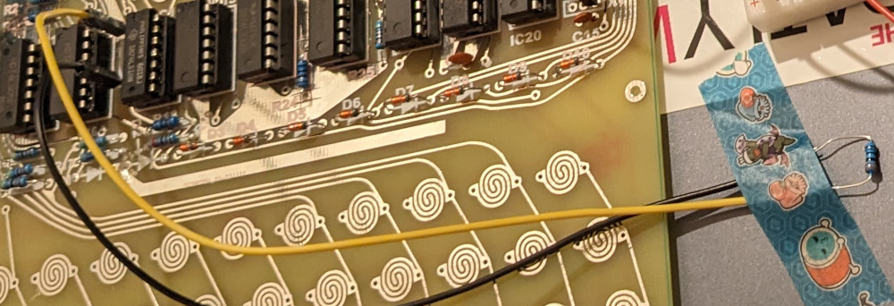
- I forgot to solder on R20. This resistor is needed in the clock circuit. Fixed using jumper wires.
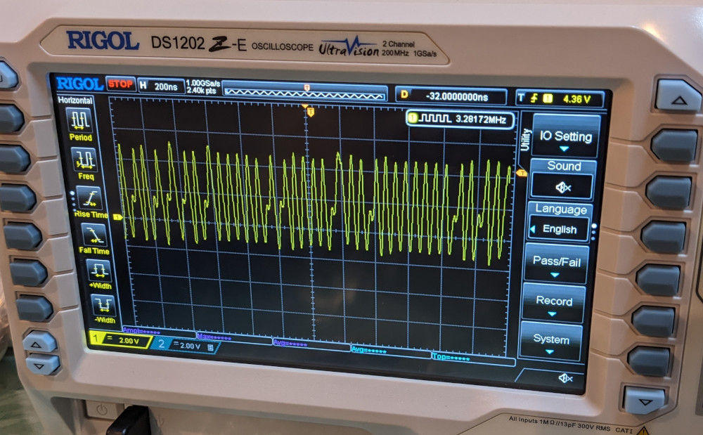
- I changed the Pico’s output pin from GPIO0 to GPIO2 and failed to re-wire. I then suspected the Z80 was bad and tested it on a breadboard with the data pins tied to ground to emulate NOPs. Eventually figured out the problem (dur). It was difficult to figure out at first because the circuitry on the PCB picked up the output from GPIO2 as noise, and amplified it to produce something like a clock signal. Except that this was a very dirty clock signal (see image below)! It is interesting that the Z80 seems to detect that the clock is a little cuckoo, and while it works for a split second, it quickly calls it quits and the address bus freezes in a random state. That seems like a useful thing to be aware of! (Could of course be that this is not an intentional feature, or that it’s just seeing a HALT instruction or something.)
- While testing the Z80 on the breadboard, I set the Pico’s clock output to 3.25 MHz. I then forgot to change it back to 6.5 MHz.
RAM problem
The 2114 RAM chips originally came out of the Commodore PET that I fixed two years ago. I removed them from the PET because they were a little faulty, but kept them because they still mostly worked. Lucky! I had three, and hoped two of them would work well enough to at least get the ZX80 booted. Well, I picked a lucky one and an unlucky one. I didn’t see anything on the composite output. (Which at the time of writing is just a hole in the PCB. The ZX80 and early versions of the ZX81 don’t produce a back porch, but that problem is somehow fixed or alleviated or otherwise rendered irrelevant inside the modulator. The problem just manifests itself when you decide that the wire leading into the modulator is now going to be composite output. Back when I was looking at the ZX81 at the computer museum in Oume, I used a 555-based circuit that I got from here to fix the problem.)
Not knowing whether it’s a RAM problem or a serious problem with the PCB, I broke out my Pico-based logic analyzer. This time I didn’t bother adding resistor dividers because all Picos I have (I think I have four) turned out to be a least a little 5V-tolerant, and I wouldn’t be using the logic analyzer for a long time.
I needed to make some minor modifications to the logic analyzer code: the reset circuit in the ZX80 uses a 220K pull-up resistor (it’s very high value because it is also a 1 second (or so) RC delay circuit), and the Pico by default has pull downs active on its input GPIOs. These pull downs are much lower in value than 220K, effectively keeping reset asserted forever. (They are surprisingly low!) So the init code now looks like this:
    stdio_init_all();
    gpio_init_mask(ALL_REGULAR_GPIO_PINS);
    gpio_set_dir_masked(ALL_REGULAR_GPIO_PINS, GPIO_IN);
    gpio_disable_pulls(TRIGGER_PIN); // default is pull down; this pull down is much higher in value the the zx80's reset circuit's pull-up and therefore holds the cpu in reset
Of course, it would probably be even better if we disabled all pulls on all GPIOs. Anyway, running the logic analyzer, I quickly found a RAM problem with bit 4.
Here is the logic analyzer output with the problematic signals:
    115       6 0283 40
    116      16 0283 2a
    117       1 0f10 2a
    118      21 0f50 00
    119       6 0284 00
    120      27 0284 0a
    121       6 0285 0a
    122      27 0285 40
    123       8 000a 40
    124      25 000a 21
    125       8 000b 21
    126      25 000b 40
The first number is just the line number, the second number is the number of times the third and fourth numbers are repeated in the logic analyzer output (which is not in sync with the clock, but much faster). You can ignore everything that is less than around 10. In the above output, we are fetching and then executing the instruction at 0x0283~0x0285. Here is the relevant assembly source:
        ld iy,04000h            ;0273   fd 21 00 40     . ! . @
        ld hl,04028h            ;0277   21 28 40        ! ( @
        ld (04008h),hl          ;027a   22 08 40        " . @
        ld (hl),080h            ;027d   36 80   6 .
        inc hl                  ;027f   23      #
        ld (0400ah),hl          ;0280   22 0a 40        " . @
        ld hl,(0400ah)          ;0283   2a 0a 40        * . @
So we can see that we are putting 0x4028 into hl, and then incrementing hl, which means that hl should now be 0x4029. The instruction at 0x280~0x282 puts hl into 0x400a, and the instruction at 0x0283~0x0285 reads it back from the same address. So we should be putting 0x4029 in there (though not shown above, we are) and should be reading 0x4029 back. But the relevant parts of the logic analyzer output are like this:
    124      25 000a 21
    126      25 000b 40
Don’t worry about this showing 000a and 000b rather than 400a and 400b. I just don’t have the higher address lines connected to the logic analyzer. We’re reading back 0x4021! That’s missing the fourth bit. So I put in the other RAM chip and bam! I see a lovely 15.something KHz signal on the through hole that would normally be occupied by one of the modulator’s leads! (Well, actually I saw a 7.65 KHz signal because I forgot to change the Pico’s clock output back to 6.5 MHz, but while that was very puzzling for a bit, it was very easy to fix.)
There’s a problem though: I’m not able to press keys like ” and many other shifted keys. I haven’t properly looked into that problem yet. However, I did do a quick internet search and found someone with the same problem:
For example, all of 1 to 0 keys work but shifted, only 1 and 0 work. Some other shifted keys don’t work but there doesn’t seem to be a consistent pattern on each row. The display still flickers when say shift 2 or shift 9 (or other combinations) is pressed, just nothing else happens.
https://sinclairzxworld.com/viewtopic.php?p=32893&sid=b108eefd0c71a1bedd148b3049db2673#p32893
But their problem was apparently caused by using super long wires on their keyboard. I’m not doing that as far as I know?!
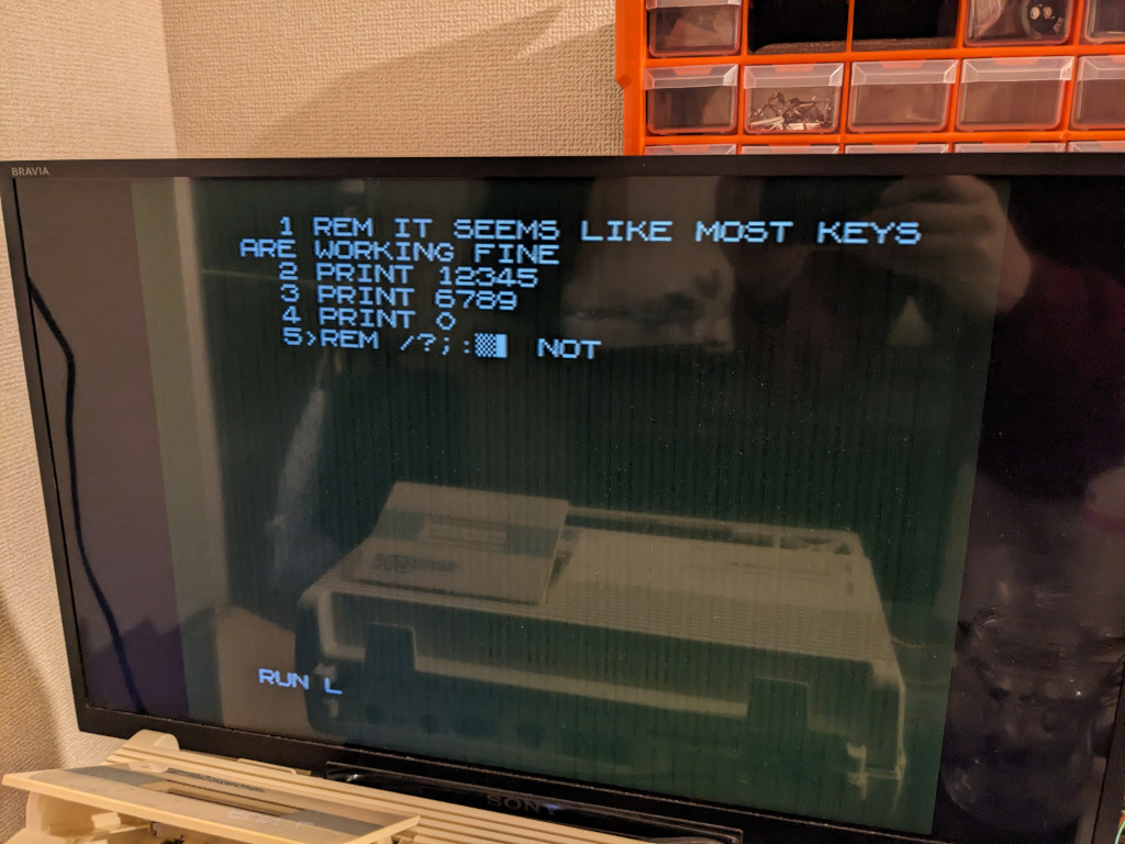
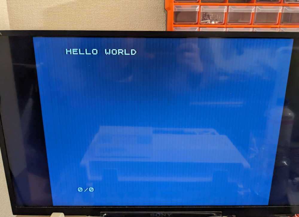
As my EEPROM is currently mounted on a breadboard and my EEPROM is 512 KB while the ZX80’s ROM is just 4 KB, I have plenty of space left. So I put the ZX81 ROM image at address 0x10000, which means I just need to change the wire on the EEPROM’s A16 pin from 0V to 5V to change to that ROM. And it works too! Plus, the keyboard layout is different, which means I’m able to access the ” key and print out a proper message rather than just numbers:
To do
- Solder crystal oscillator (when I get it) and R20, and maybe headphone/microphone jacks, etc.
- Backporch generator
- Make a proper ROM adapter?
- Get all shifted keys to work
- RAM expansion
- Try to load some software
- Make the keyboard more ergonomic
- Maybe get some kind of case
KiCad / Gerber files
Here are the SVG and KiCad files, with the above mentioned shorting issues most likely fixed. Some important notes:
- I do not have permission from Grant Searle nor from the copyright holders of the original ZX80 PCB to post anything like this, and if either of these parties asks me to take my files down, I intend to comply swiftly. (I’d just need to be sure that you are who you claim to be. I apologize in advance for any grievance caused and will apologize again if grievance is actually caused.)
- I used Grant Searle’s replica foils as a base and traced them in Inkscape. I performed some manual and some automated tweaks. This version of the board is likely a less faithful replica of the original board than Grant Searle’s foils. (I don’t think anything’s shifted more than even 1 mm though. Though maybe the holes are quite different. I didn’t encounter any problems with the drill holes while soldering though.)
- I haven’t tested (i.e. manufactured) this version of the KiCad files, I have only ordered one set of the ZX80 boards, with the shorted pins. This issue should be fixed now, and I hope I didn’t add any new issues.
Update 2025-01-19
I haven’t updated this post in a while; in the meantime the above TODO list has changed as follows:
Solder crystal oscillator (when I get it) and R20, and maybe headphone/microphone jacks, etc.Very low-hanging fruit, done. The headphone/microphone jacks I got had thicker pins that I had expected, and I had to widen the holes in the PCB a little bit.Backporch generatorDone. Though it’s implemented on a breadboard. I just used the exact same circuit that I used in my post on the ZX81 repair, the 555-based one from http://zx.zigg.net/misc-projects/.- Make a proper ROM adapter? ← Not done yet
- Get all shifted keys to work ← While it’s already almost one year ago, I had a good look at what’s going on. I’m betting that it’s my breadboard-based ROM adapter that is adding capacitance into the circuit. Together with the resistors (the ones positioned between the ICs and the keyboard), I observed a long RC delay that prevents signals from the key press to rise/fall (can’t remember which) in time. I used lower value for the aforementioned resistors but couldn’t get all keys to work while using the 4 KB (ZX80) ROM. However, using the ZX81 ROM, it looks like the programmers gave us more time and everything just works (I already replaced the resistors so not sure if it worked with the original ones). Thus I’m usually using the ZX81 ROM.
- RAM expansion ← Not done yet
Try to load some software← Works- Make the keyboard more ergonomic ← Not done yet
- Maybe get some kind of case ← Not done yet
Relatedly, I found someone who happened to do something exactly like this right around the same time as me. He published his files as a shared project on PCBWay: https://www.pcbway.com/project/shareproject/ZX80_SINCLAIR_REPLICA_066e073d.html. Amazing that somebody else decided to do this :O