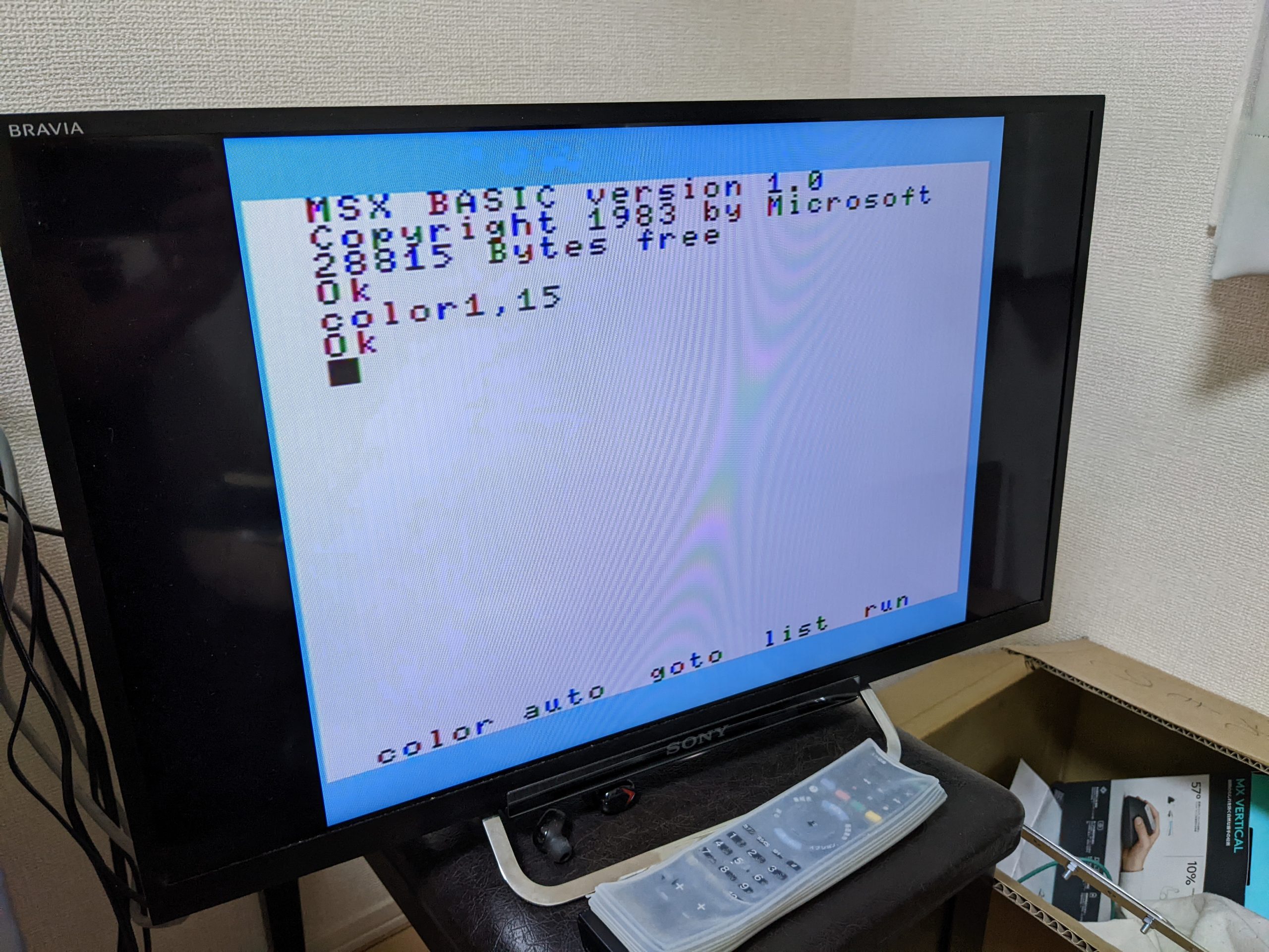
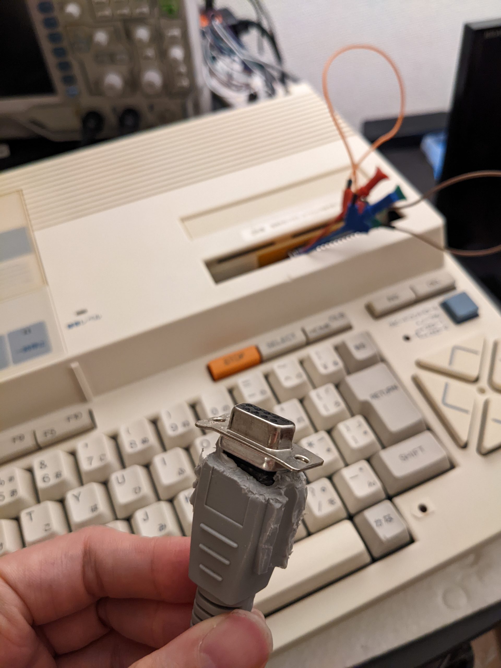
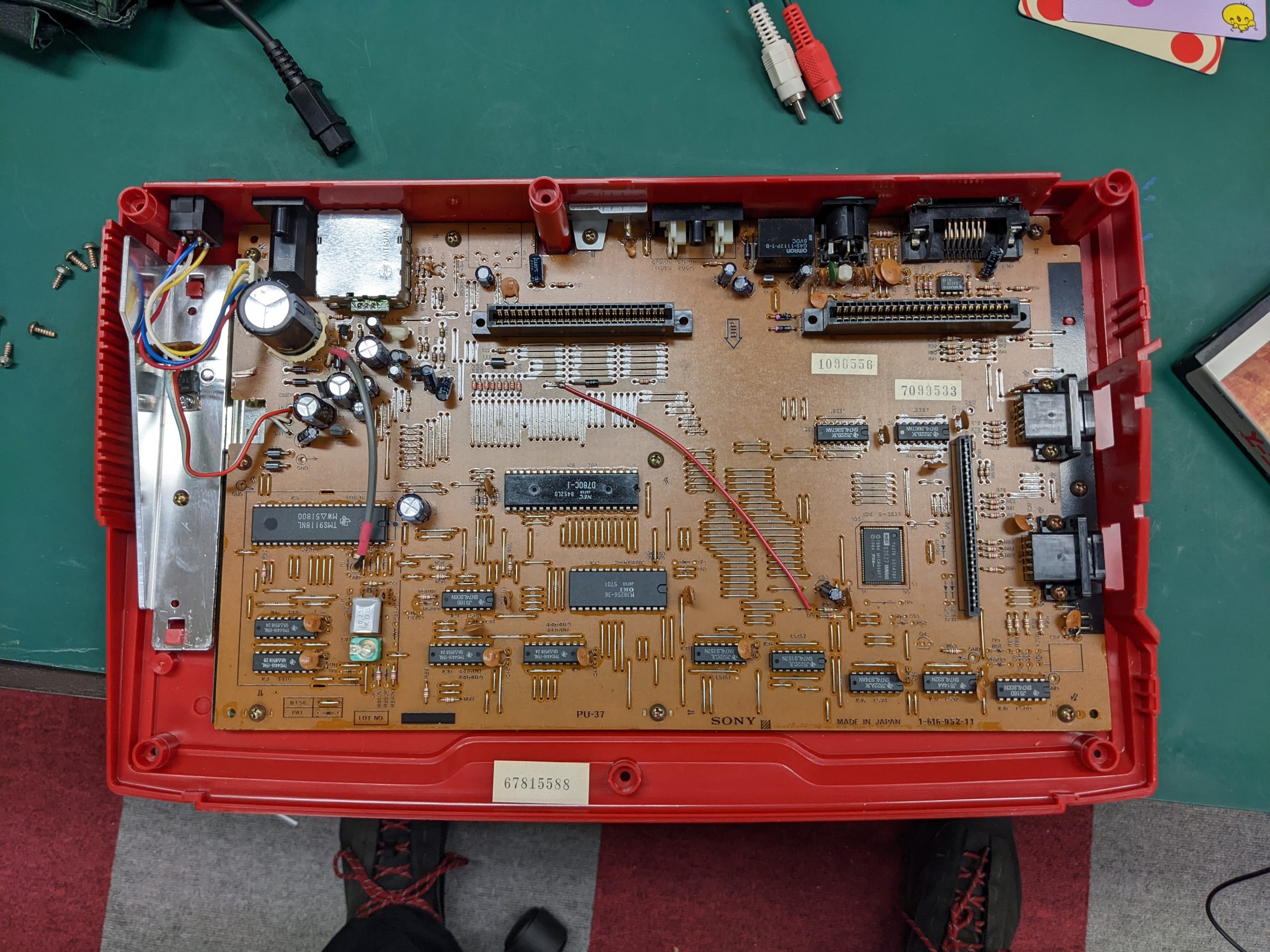
My Hitachi MB-H2 MSX machine has an analog RGB port that produces a 15.6 KHz CSYNC (combined horizontal and vertical) signal and analog voltages indicating how red, green or yellow things are.
I recently unearthed my old LCD from 2006 or so and decided to see if I could get it to sync if I just massaged the CSYNC signal a bit to bring it to TTL levels and connected a VGA cable.
(Technical details: when you connect a VGA cable to a monitor that is powered on, you will often first of all see a message like “Cable not connected”. To get past that problem, you first have to ground a certain pin on the VGA connector. I found that female Dupont connectors fit reasonably well on male VGA connectors so I just used a cable with female Dupont connectors on both ends to connect the two relevant pins. I’m not sure if it’s the same pin on all monitors. You can find the pin by looking for a pin that should be GND according to the VGA pinout but actually has some voltage on it. Don’t blame me if you break your Dupont connectors by following this advice.)
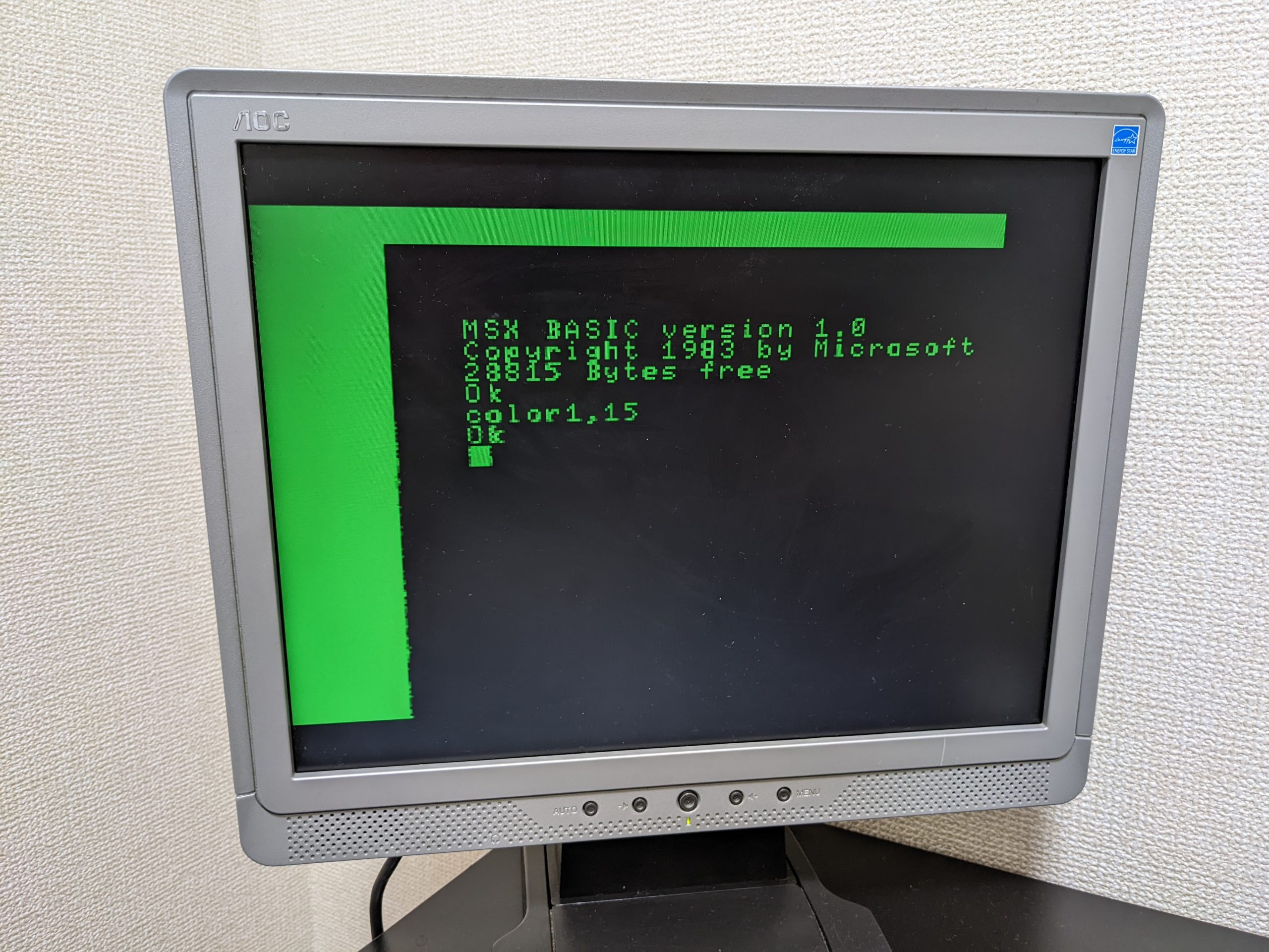
Unfortunately, that didn’t work. I got “Input not supported”, and I am reasonably sure that is because my monitor doesn’t support 15 KHz signals. Aw, why’d I even bother taking it out of storage?
So what do we do… Well there is this library (PicoVGA) that produces VGA signals using the Raspberry Pi Pico’s PIOs. Raspberry Pi Picos are extremely cheap, just about 600 yen per piece where I am.
Damn, I’ve seen this in videos, but seeing this in real life, a tiny, puny microcontroller generating fricking VGA signals! Amazing. Just last year I was playing around with monochrome composite output on an Arduino Nano, and even that was super impressive to me! (Cue people reading this 20 years in the future and laughing at the silly dude with the retro microcontroller from year-of-the-pandemic 2020. I’m sure microcontrollers in the 2040s will have 32 cores and dozens of pins with built-in 1 GHz DACs and ADCs and mains voltage tolerance, and will be able to generate a couple streams of 4K video ;D)
Some boring technical notes I took before embarking on the project, feel free to skip this section
Is the Pico’s VGA library magic? Yes, definitely. Can we add our own magic to simultaneously capture video and output it via the VGA library?
It sure looks like it! Why?
- The Pico has two CPU cores, and the VGA library uses just one of them, the second core
- Dual-core microcontroller, that’s craziness
- We may be able to use the second core a little bit anyway (“If the second core is not very busy (e.g. when displaying 8-bit graphics that are simply transferred using DMA transfer), it can also be used for the main program work.”)
- We will indeed be working with 8-bit graphics simply transferred using DMA
- The Pico has two PIO controllers, and the VGA library uses just one (“The display of the image by the PicoVGA library is performed by the PIO processor controller. PIO0 is used. The other controller, PIO1, is unused and can be used for other purposes.”)
However:
- We possibly won’t be able to use DMA all that much (“Care must also be taken when using DMA transfer. DMA is used to transfer data to the PIO. Although the transfer uses a FIFO cache, using a different DMA channel may cause the render DMA channel to be delayed and thus cause the video to drop out. A DMA overload can occur, for example, when a large block of data in RAM is transferred quickly. However, the biggest load is the DMA transfer of data from flash memory. In this case, the DMA channel waits for data to be read from flash via QSPI and thus blocks the DMA render channel.”)
- If we use PIO and DMA for capturing video-in, we might run into trouble there
- However, using DMA to capture and another DMA transfer to transfer the data to VGA out sounds somewhat inefficient; maybe it’s possible to directly transfer from capture PIO to VGA PIO? Would require modifications to the VGA library, which doesn’t sound so great right now (we didn’t do this)
That said, it’s likely that capturing without the use of PIO would be fast enough, generally speaking.
The “pixel clock” for a 320×200 @ 60 Hz signal is between 4.944 and 6 MHz according to https://tomverbeure.github.io/video_timings_calculator (select 320×200 / 60 in the drop-down menu), depending on some kind of mode that I don’t know anything about.
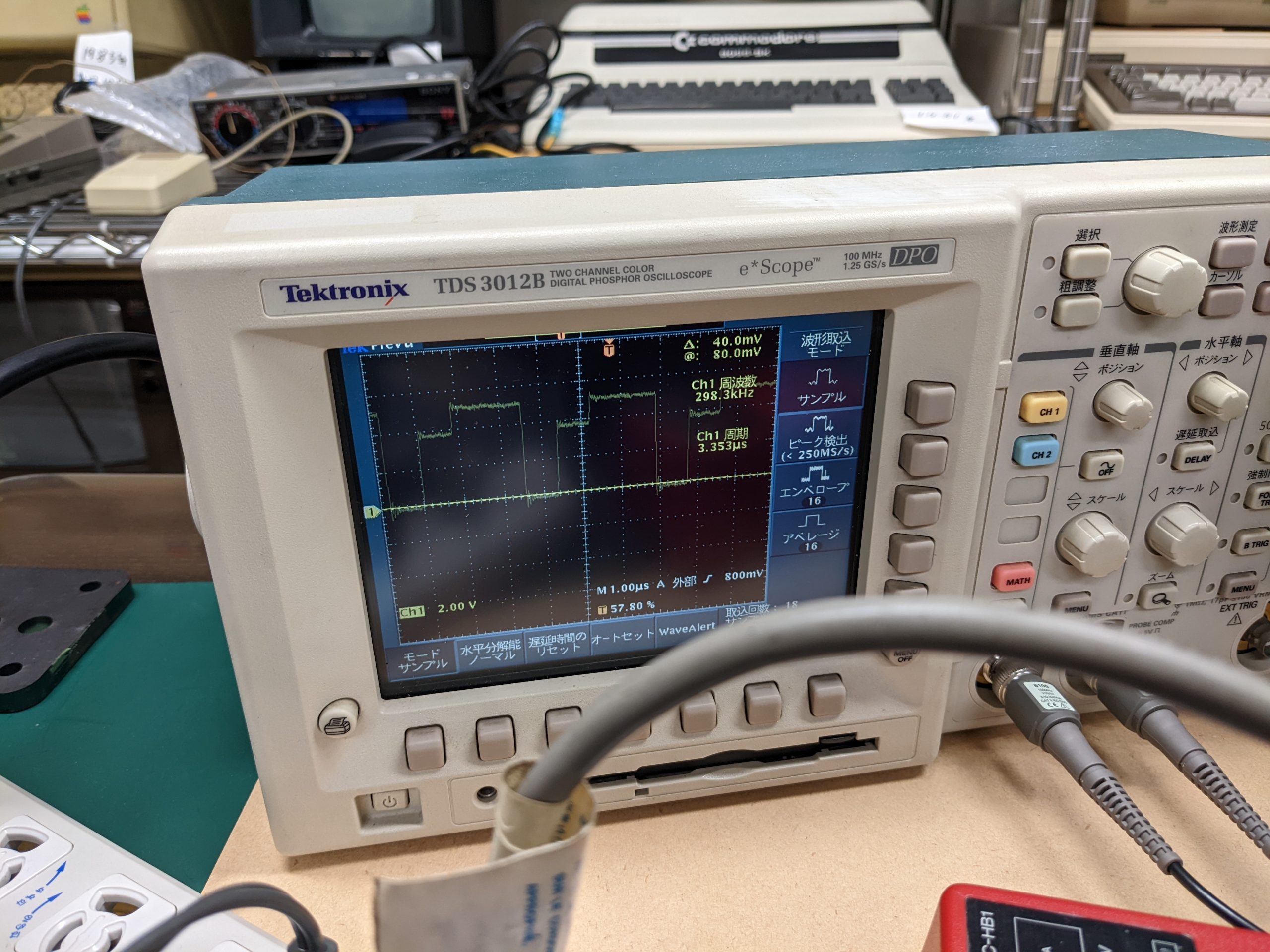
According to our oscilloscope capture of a single pixel on one of the color channels (DS1Z_QuickPrint22.png), we get about 5.102 MHz. Let’s take that value. We’ll hopefully be able to calculate the exact value at some point. (Yeah, the TMS59918A/TMS59928A/TMS59929A datasheet actually (almost) mentions the exact value! “The VDP is designed to operate with a 10.738635 (± 0.005) MHz crystal”, “This master clock is divided by two to generate the pixel clock (5.3 MHz)”. So it’s 5.3693175 MHz, thank you very much.)
This means that we have to be able to capture at exactly that frequency. From our previous experimental logic analyzer (which doesn’t use PIO) we were more than capable of capturing everything going on with our Z80 CPU — we had multiple samples of every single state the CPU happened to be in, and the CPU ran at 3.58 MHz. (However, if the VGA library chooses to set the CPU to use a lower clock frequency, we may run into problems. It’s possible to prevent the library from adjusting the clock frequency, but maybe that will impact image quality.) The main part of the code looked like this:
for (i = 0; i < LOGIC_BUFFER_LEN; i++) {
    logic_buffer[i] = gpio_get_all() & ALL_REGULAR_GPIO_PINS;
}
To capture video, we’d like to post-process our capture just a little bit, to convert it to 3-3-2 RGB. Or we could post-process our capture during VSYNC, but that would be a rather tight fit, with only 1.2 ms to work with. (Actually, our signal’s VSYNC pulse is even shorter than that, but there’s nothing on the RGB pins for a while before and after that.)
So our loop might look like this. (Note, the code I ended up writing looks reasonably similar to this, which is why I’m including this here.)
for (x = 0; x < 320; x++) {
    pixel = gpio_get_all();
    red = msb_table_inverted[((pixel & R_MASK) >> R_SHIFT) << R_SHIFT];
    green = msb_table_inverted[((pixel & G_MASK) >> G_SHIFT) << G_SHIFT];
    blue = msb_table_inverted[((pixel & B_MASK) >> B_SHIFT) << B_SHIFT];
    capture[y][x] = red | (green << 3) | (blue << 6);
}
Where msb_table_inverted is a lookup table to convert our raw GPIO input to the proper R/G/B values. This depends on how we do the analog to digital conversion, so the loop might look slightly different in the end.
Well, how likely is it that this will produce a perfectly synced capture? About 0% in my opinion. If we’re too fast, we’ll get a horizontally compressed image. If we’re too slow, the image will be wider than it should be, and more importantly, cut off on the right side.
In the first case, we may be able to improve the situation by adding the right amount of NOPs.
In the second case, we could reduce the amount of on-the-fly post-processing, and do stuff during HBLANK or VBLANK instead.
In addition, we might miss a few pixels on the left side if we can’t begin capturing immediately when we get our HSYNC interrupt. How likely is this to succeed? It might work, I think.
The PIOs can also be used without DMA. (Instead of using DMA, we’d use functions like pio_sm_get_blocking().) With PIO, we can get perfect timing, which would be really great to have. We can’t off-load any arithmetic or bit twiddling operations, the PIOs don’t have that. So let’s dig in and run some experiments.
Implementation
The pico_examples repository has a couple of PIO examples. The PicoVGA library has a hello world example. I thought the logic_analyser example in pico_examples looked like a good start. It’s really quite amazing.
- You can specify the number of samples you’d like to read (const uint CAPTURE_N_SAMPLES = 96)
- You can specify the number of pins you’d like to sample from (const uint CAPTURE_PIN_COUNT = 2)
- You can specify the frequency you’d like to read at (logic_analyser_init(pio, sm, CAPTURE_PIN_BASE, CAPTURE_PIN_COUNT, 1.f), where “1.f” is a divider of the system clock. I.e., this will capture at system clock speed. We can specify a float number here.)
- The PIO input is (mostly?) independent from what else you have going on on that pin, so the code of course proceeds to configure a PWM signal on a pin, and to capture from that same pin. Bonkers!
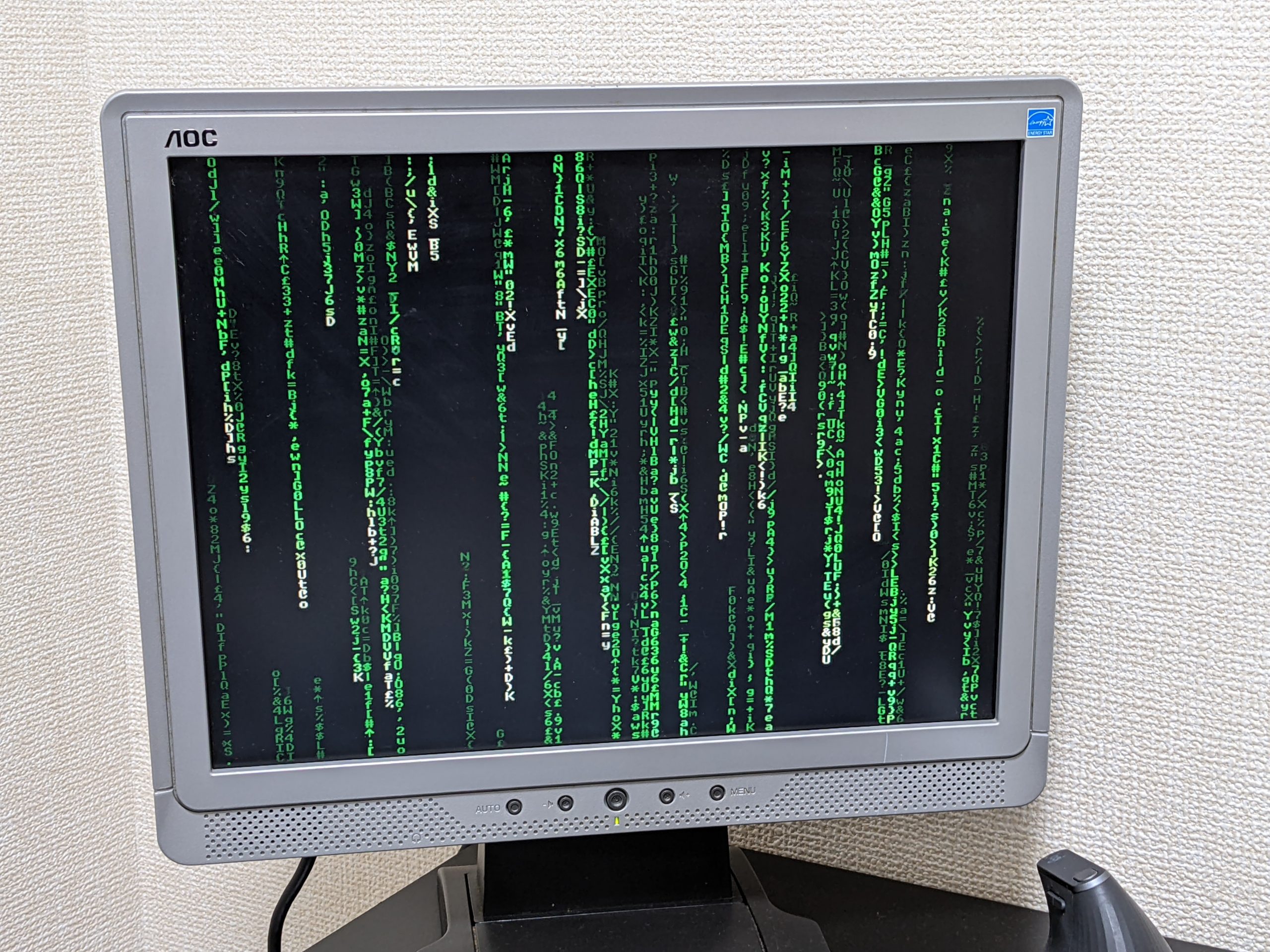
Well, let’s cut to the chase, shall we? I took parts of the logic_analyser code to capture the input from RGB, then wrote some code to massage the captured data a little bit, and then output everything using PicoVGA at a higher resolution. After some troubleshooting, I got a readable signal!
However, my capture has wobbly scanlines. Which is why there might be a part 2. And since it’s wobbly, I spent even less effort on the analog to digital conversion than I’d originally planned, which was already rather “poor man” (more on that later, because the code assumes that circuit exists).
I’m triggering the capture by looking for a positive to negative transition. (That’s already two out of the three instructions my PIO program consists of, one to wait for positive, one to wait for negative.) I currently don’t really know why my scanlines are wobbly. I had a few looks with the oscilloscope to see if there’s anything wrong in my circuit that converts CSYNC to TTL levels — for example, slow response from the transistor. But I didn’t find anything so far. :3 It’s of course entirely possible that the source signal is wonky. I’ve never had a chance to connect my MSX to a monitor that supports 15 KHz signals. (Now that’s a major TODO right there.) Of course there are other ways to check if the signal is okay.
We could also (hopefully) get rid of the wobbling by only paying attention to the VSYNC and timing scanlines ourselves, for example by generating them using the Pico’s PWM. As seen in the original logic_analyser.c code! But that’s something for part 2 I guess.
BTW, it’s unlikely that the wobbliness is being caused by a problem with the code or resource contention. I tested this by switching the capture to an off-screen buffer after a few seconds. The screen displayed the last frame captured into the real framebuffer, and was entirely static. I.e., I added code like this into the main loop (which you will see below):
+        if (j > 600) {
+            rgb_buf = fake_rgb_buf;
+            gpio_put(PICO_DEFAULT_LED_PIN, true);
+        } else {
+            j++;
+        }
Poor-man’s ADC
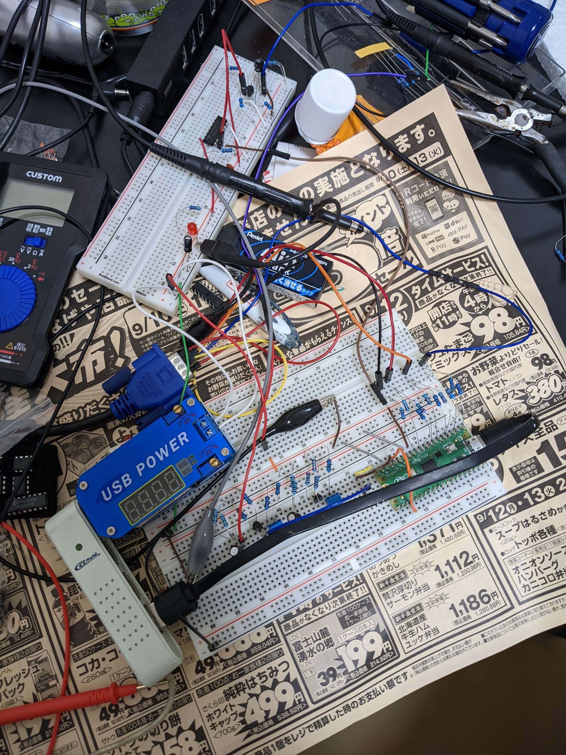
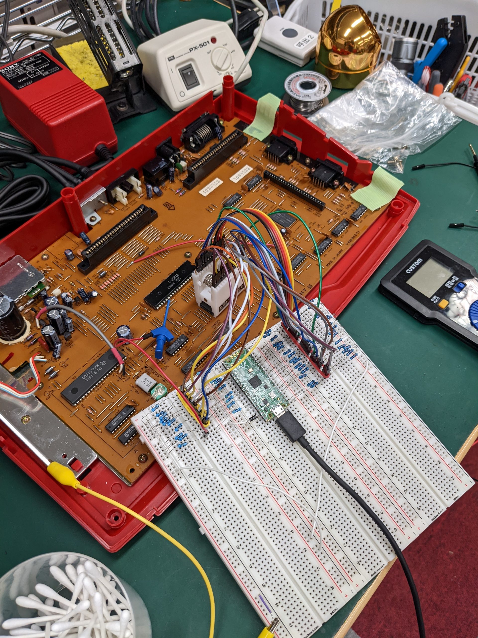
What I actually planned to do: the program I wrote expects four different levels of red, green, and blue. There are three pins per color, and if all pins of a color are 0, that means that color is 0, if only one is 1, that’s still quite dark, if two are 1, that’s somewhat bright, and if all three are 1, then that’s bright. The program then converts that into two bits (0, 1, 2, 3); PicoVGA works with 8-bit colors, 3 bits for red, 3 bits for green, 2 bits for blue. That means that we can capture all the blue we need, and for red and green we could scale the numbers a bit. However, I shelved that plan for now, because I don’t even have enough potentiometers at the moment, and if the signal is as wobbly as it is, that’s just putting lipstick on a pig. Instead, I just took a single color (blue, just because that was less likely to short my MacGyver wiring), and feed that into all colors’ “bright” pin.
As my MSX’s RGB signal voltages are a bit funky (-0.7 to 0.1 IIRC), I converted that to something the Pico can understand using a simple class A-kinda amplifier. The signal gets inverted by this circuit, but that’s fine for a POC. Completely blue will be black, and vice versa.
So here’s the code:
#include "include.h"
#include <stdio.h>
#include <stdlib.h>
#include "pico/stdlib.h"
#include "hardware/pio.h"
#include "hardware/dma.h"
#include "hardware/structs/bus_ctrl.h"
// Some logic to analyse:
#include "hardware/structs/pwm.h"
const uint CAPTURE_PIN_BASE = 9;
const uint CAPTURE_PIN_COUNT = 10; // CSYNC, 3*R, 3*G, 3*B
const float PIXEL_CLOCK = 5369.3175f; // datasheet (TMS9918A_TMS9928A_TMS9929A_Video_Display_Processors_Data_Manual_Nov82.pdf) page 3-8 / section 3.6.1 says 5.3693175 MHz (10.73865/2)
// from same page on datasheet
// HORIZONTAL PATTERN OR MULTICOLOR TEXT
// HORIZONTAL ACTIVE DISPLAY 256 240
// RIGHT BORDER 15 25
// RIGHT BLANKING 8 8
// HORIZONTAL SYNC 26 26
// LEFT BLANKING 2 2
// COLOR BURST 14 14
// LEFT BLANKING 8 8
// LEFT BORDER 13 19
// TOTAL 342 342
const uint INPUT_VIDEO_WIDTH = 308; // left blanking + color burst + left blanking + left border + active + right border
// VERTICAL LINE
// VERTICAL ACTIVE DISPLAY 192
// BOTTOM BORDER 24
// BOTTOM BLANKING 3
// VERTICAL SYNC 3
// TOP BLANKING 13
// TOP BORDER 27
// TOTAL 262
const uint INPUT_VIDEO_HEIGHT = 240; // top blanking + top border + active + 1/3 of bottom border
const uint INPUT_VIDEO_HEIGHT_OFFSET_Y = 40; // ignore top 40 (top blanking + top border) scanlines
// we're capturing everything there is to see on the horizontal axis, but throwing out most of the border on the vertical axis
// NOTE: other machines probably have different blanking/border periods
const uint CAPTURE_N_SAMPLES = INPUT_VIDEO_WIDTH;
const uint OUTPUT_VIDEO_WIDTH = 320;
const uint OUTPUT_VIDEO_HEIGHT = 200;
static_assert(OUTPUT_VIDEO_WIDTH >= INPUT_VIDEO_WIDTH);
static_assert(OUTPUT_VIDEO_HEIGHT >= INPUT_VIDEO_HEIGHT-INPUT_VIDEO_HEIGHT_OFFSET_Y);
uint offset; // Lazy global variable; this holds the offset of our PIO program
// Framebuffer
ALIGNED u8 rgb_buf[OUTPUT_VIDEO_WIDTH*OUTPUT_VIDEO_HEIGHT];
static inline uint bits_packed_per_word(uint pin_count) {
// If the number of pins to be sampled divides the shift register size, we
// can use the full SR and FIFO width, and push when the input shift count
// exactly reaches 32. If not, we have to push earlier, so we use the FIFO
// a little less efficiently.
const uint SHIFT_REG_WIDTH = 32;
return SHIFT_REG_WIDTH - (SHIFT_REG_WIDTH % pin_count);
}
void logic_analyser_init(PIO pio, uint sm, uint pin_base, uint pin_count, float div) {
// Load a program to capture n pins. This is just a single `in pins, n`
// instruction with a wrap.
uint16_t capture_prog_instr[3];
capture_prog_instr[0] = pio_encode_wait_gpio(false, pin_base);
capture_prog_instr[1] = pio_encode_wait_gpio(true, pin_base);
capture_prog_instr[2] = pio_encode_in(pio_pins, pin_count);
struct pio_program capture_prog = {
.instructions = capture_prog_instr,
.length = 3,
.origin = -1
};
offset = pio_add_program(pio, &capture_prog);
// Configure state machine to loop over this `in` instruction forever,
// with autopush enabled.
pio_sm_config c = pio_get_default_sm_config();
sm_config_set_in_pins(&c, pin_base);
sm_config_set_wrap(&c, offset+2, offset+2); // do not repeat pio_encode_wait_gpio instructions
sm_config_set_clkdiv(&c, div);
// Note that we may push at a < 32 bit threshold if pin_count does not
// divide 32. We are using shift-to-right, so the sample data ends up
// left-justified in the FIFO in this case, with some zeroes at the LSBs.
sm_config_set_in_shift(&c, true, true, bits_packed_per_word(pin_count)); // push when we have reached 32 - (32 % pin_count) bits (27 if pin_count==9, 30 if pin_count==10)
sm_config_set_fifo_join(&c, PIO_FIFO_JOIN_RX); // TX not used, so we can use everything for RX
pio_sm_init(pio, sm, offset, &c);
}
void logic_analyser_arm(PIO pio, uint sm, uint dma_chan, uint32_t *capture_buf, size_t capture_size_words,
uint trigger_pin, bool trigger_level) {
pio_sm_set_enabled(pio, sm, false);
// Need to clear _input shift counter_, as well as FIFO, because there may be
// partial ISR contents left over from a previous run. sm_restart does this.
pio_sm_clear_fifos(pio, sm);
pio_sm_restart(pio, sm);
dma_channel_config c = dma_channel_get_default_config(dma_chan);
channel_config_set_read_increment(&c, false);
channel_config_set_write_increment(&c, true);
channel_config_set_dreq(&c, pio_get_dreq(pio, sm, false)); // pio_get_dreq returns something the DMA controller can use to know when to transfer something
dma_channel_configure(dma_chan, &c,
capture_buf, // Destination pointer
&pio->rxf[sm], // Source pointer
capture_size_words, // Number of transfers
true // Start immediately
);
pio_sm_exec(pio, sm, pio_encode_jmp(offset)); // just restarting doesn't jump back to the initial_pc AFAICT
pio_sm_set_enabled(pio, sm, true);
}
void blink(uint32_t ms=500)
{
gpio_put(PICO_DEFAULT_LED_PIN, true);
sleep_ms(ms);
gpio_put(PICO_DEFAULT_LED_PIN, false);
sleep_ms(ms);
}
// uint8_t msb_table_inverted[8] = { 3, 3, 3, 3, 2, 2, 1, 0 };
uint8_t msb_table_inverted[8] = { 0, 1, 2, 2, 3, 3, 3, 3 };
void post_process(uint8_t *rgb_bufy, uint32_t *capture_buf, uint buf_size_words)
{
uint16_t i, j, k;
uint32_t temp;
for (i = 8, j = 0; i < buf_size_words; i++, j += 3) { // start copying at pixel 24 (8*3) (i.e., ignore left blank and color burst, exactly 24 pixels).
temp = capture_buf[i] >> (2+1); // 2: we're only shifting in 30 bits out of 32, 1: ignore csync
rgb_bufy[j] = msb_table_inverted[temp & 0b111]; // red
rgb_bufy[j] |= (msb_table_inverted[(temp & 0b111000) >> 3] << 3); // green
rgb_bufy[j] |= (msb_table_inverted[(temp & 0b111000000) >> 6] << 6); // blue
temp >>= 10; // go to next sample, ignoring csync
rgb_bufy[j+1] = msb_table_inverted[temp & 0b111]; // red
rgb_bufy[j+1] |= (msb_table_inverted[(temp & 0b111000) >> 3] << 3); // green
rgb_bufy[j+1] |= (msb_table_inverted[(temp & 0b111000000) >> 6] << 6); // blue
temp >>= 10; // go to next sample, ignoring csync
rgb_bufy[j+2] = msb_table_inverted[temp & 0b111]; // red
rgb_bufy[j+2] |= (msb_table_inverted[(temp & 0b111000) >> 3] << 3); // green
rgb_bufy[j+2] |= (msb_table_inverted[(temp & 0b111000000) >> 6] << 6); // blue
}
}
int main()
{
uint16_t i, y;
gpio_init(PICO_DEFAULT_LED_PIN);
gpio_init(CAPTURE_PIN_BASE);
gpio_set_dir(PICO_DEFAULT_LED_PIN, GPIO_OUT);
gpio_set_dir(CAPTURE_PIN_BASE, GPIO_IN);
blink();
// initialize videomode
Video(DEV_VGA, RES_CGA, FORM_8BIT, rgb_buf);
blink();
// We're going to capture into a u32 buffer, for best DMA efficiency. Need
// to be careful of rounding in case the number of pins being sampled
// isn't a power of 2.
uint total_sample_bits = CAPTURE_N_SAMPLES * CAPTURE_PIN_COUNT;
total_sample_bits += bits_packed_per_word(CAPTURE_PIN_COUNT) - 1;
uint buf_size_words = total_sample_bits / bits_packed_per_word(CAPTURE_PIN_COUNT);
uint32_t *capture_buf0 = (uint32_t*)malloc(buf_size_words * sizeof(uint32_t));
hard_assert(capture_buf0);
uint32_t *capture_buf1 = (uint32_t*)malloc(buf_size_words * sizeof(uint32_t));
hard_assert(capture_buf1);
blink();
// Grant high bus priority to the DMA, so it can shove the processors out
// of the way. This should only be needed if you are pushing things up to
// >16bits/clk here, i.e. if you need to saturate the bus completely.
// (Didn't try this)
// bus_ctrl_hw->priority = BUSCTRL_BUS_PRIORITY_DMA_W_BITS | BUSCTRL_BUS_PRIORITY_DMA_R_BITS;
PIO pio = pio1;
uint sm = 0;
uint dma_chan = 8; // 0-7 may be used by VGA library (depending on resolution)
logic_analyser_init(pio, sm, CAPTURE_PIN_BASE, CAPTURE_PIN_COUNT, (float)Vmode.freq/PIXEL_CLOCK);
blink();
// 1) DMA in 1st scan line, wait for completion
// 2) DMA in 2nd scan line, post-process previous scan line, wait for completion
// 3) DMA in 3rd scan line, post-process previous scan line, wait for completion
// ...
// n) Post-process last scanline
// I'm reasonably sure we have enough processing power to post-process scanlines in real time, we should have about 80 us.
// At 126 MHz each clock cycle is about 8 ns, so we have 10000 instructions to process about 320 bytes, or 31.25 instructions per byte.
while (true) {
// "Software-render" vsync detection... I.e., wait for low on csync, usleep for hsync_pulse_time+something, check if we're still low
// If we are, that's a vsync pulse!
// This works well enough AFAICT
while (true) {
while(gpio_get(CAPTURE_PIN_BASE)); // wait for negative pulse on csync
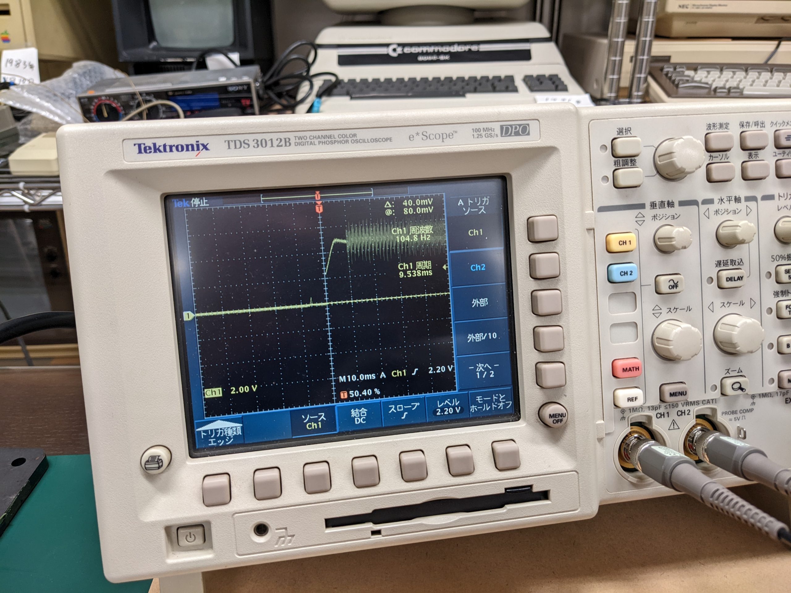
sleep_us(10); // hsync negative pulse is about 4.92 us according to oscilloscope, so let's wait a little longer than 4.92 us
if (!gpio_get(CAPTURE_PIN_BASE)) // we're still low! this must be a vsync pulse
break;
}
for (y = 0; y <= INPUT_VIDEO_HEIGHT_OFFSET_Y; y ++) { // capture and throw away first 40 scanlines, capture without throwing away 41st scanline
logic_analyser_arm(pio, sm, dma_chan, capture_buf0, buf_size_words, CAPTURE_PIN_BASE, true);
dma_channel_wait_for_finish_blocking(dma_chan);
}
for (y = 1; y < (INPUT_VIDEO_HEIGHT-INPUT_VIDEO_HEIGHT_OFFSET_Y)-1; y += 2) {
logic_analyser_arm(pio, sm, dma_chan, capture_buf1, buf_size_words, CAPTURE_PIN_BASE, true);
post_process(rgb_buf + (y-1)*OUTPUT_VIDEO_WIDTH, capture_buf0, buf_size_words);
dma_channel_wait_for_finish_blocking(dma_chan);
logic_analyser_arm(pio, sm, dma_chan, capture_buf0, buf_size_words, CAPTURE_PIN_BASE, true);
post_process(rgb_buf + y*OUTPUT_VIDEO_WIDTH, capture_buf1, buf_size_words);
dma_channel_wait_for_finish_blocking(dma_chan);
}
post_process(rgb_buf + (y-2)*OUTPUT_VIDEO_WIDTH, capture_buf0, buf_size_words);
}
}Replace vga_hello/src/main.cpp with the above file and recompile (make program.uf2). Maybe this post will help if you are on something that isn’t Windows and can’t get this to compile.
Explanation
The PIO program is generated in the logic_analyser_init function. Here it is again:
    capture_prog_instr[0] = pio_encode_wait_gpio(false, pin_base);
    capture_prog_instr[1] = pio_encode_wait_gpio(true, pin_base);
    capture_prog_instr[2] = pio_encode_in(pio_pins, pin_count);
    struct pio_program capture_prog = {
            .instructions = capture_prog_instr,
            .length = 3,
            .origin = -1
    };
First we wait for a “false” (low) signal. Then a “true” (high) signal. Then we read. Okay… but that doesn’t make any sense, does it?
No, it doesn’t, but maybe with the following bit of code:
sm_config_set_wrap(&c, offset+2, offset+2); // do not repeat pio_encode_wait_gpio instructionssm_config_set_wrap is used to tell the PIOs how to loop the PIO program. And in this case, we loop after we have executed the instruction at offset+2, and we jump to offset+2. The instruction at offset+2 is the “in” instruction. That is, we just keep executing the “in” instruction, except the first time. The first time, we wait for low on CSYNC, then wait for high on CSYNC, and then (as this state means that the CSYNC pulse is over) we keep reading as fast as we can (at the programmed PIO speed).
Results
Let’s take a look at the results. Remember, we’re converting to monochrome, and only looking at the blue channel. Remember that our super lazy “analog frontend” is super lazy, and the potentiometer has to be fine-tuned to get to a sweet spot that allows everything on the screen to be displayed.
Actually the HBLANK front porches are gone now after I fixed a typo in the code. But it’s still quite wobbly. Maybe not quite as wobbly as in the above video?
What’s the pen and the eraser doing here? TBH my eyes just tend to filter out junk after a while. So stuff just sort of becomes part of the scenery.
Minor update
Fixing a typo in the code (already fixed above as it made no sense to leave it there) fixed up the signal quite a bit. I also added buttons to fine-tune the pixel clock. This stabilizes the signal significantly. However, hopefully mostly due to the fact that our analog frontend is a bit lame, we get a somewhat fuzzy image, where some pixels change between black and white. I am somewhat tempted to build out the analog frontend properly but before that I think I’ll try my hand at digital RGB, more on that in a later post.
Anyway, here’s the updated code for analog input, with support for two buttons to fine-tune the pixel clock:
#include "include.h"

#include <stdio.h>
#include <stdlib.h>

#include "pico/stdlib.h"
#include "hardware/pio.h"
#include "hardware/dma.h"
#include "hardware/structs/bus_ctrl.h"

const uint CAPTURE_PIN_BASE = 9;
const uint CAPTURE_PIN_COUNT = 10; // CSYNC, 3*R, 3*G, 3*B
const uint INCREASE_BUTTON_PIN = 20;
const uint DECREASE_BUTTON_PIN = 21;

const PIO pio = pio1;
const uint sm = 0;
const uint dma_chan = 8; // 0-7 may be used by VGA library (depending on resolution)

const float PIXEL_CLOCK = 5369.3175f; // datasheet (TMS9918A_TMS9928A_TMS9929A_Video_Display_Processors_Data_Manual_Nov82.pdf) page 3-8 / section 3.6.1 says 5.3693175 MHz (10.73865/2)
// the pixel clock has a tolerance of +-0.005 (i.e. +- 5 KHz), let's add a facility to adjust our hard-coded pixel clock:
const float PIXEL_CLOCK_ADJUSTER = 0.1; // KHz

// from same page on datasheet
// HORIZONTAL                   PATTERN OR MULTICOLOR   TEXT
// HORIZONTAL ACTIVE DISPLAY    256                     240
// RIGHT BORDER                 15                      25
// RIGHT BLANKING               8                       8
// HORIZONTAL SYNC              26                      26
// LEFT BLANKING                2                       2
// COLOR BURST                  14                      14
// LEFT BLANKING                8                       8
// LEFT BORDER                  13                      19
// TOTAL                        342                     342

const uint INPUT_VIDEO_WIDTH = 308; // left blanking + color burst + left blanking + left border + active + right border

// VERTICAL                     LINE
// VERTICAL ACTIVE DISPLAY      192
// BOTTOM BORDER                24
// BOTTOM BLANKING              3
// VERTICAL SYNC                3
// TOP BLANKING                 13
// TOP BORDER                   27
// TOTAL                        262

const uint INPUT_VIDEO_HEIGHT = 240; // top blanking + top border + active + 1/3 of bottom border
const uint INPUT_VIDEO_HEIGHT_OFFSET_Y = 40; // ignore top 40 (top blanking + top border) scanlines
// we're capturing everything there is to see on the horizontal axis, but throwing out most of the border on the vertical axis
// NOTE: other machines probably have different blanking/border periods

const uint CAPTURE_N_SAMPLES = INPUT_VIDEO_WIDTH;

const uint OUTPUT_VIDEO_WIDTH = 320;
const uint OUTPUT_VIDEO_HEIGHT = 200;

static_assert(OUTPUT_VIDEO_WIDTH >= INPUT_VIDEO_WIDTH);
static_assert(OUTPUT_VIDEO_HEIGHT >= INPUT_VIDEO_HEIGHT-INPUT_VIDEO_HEIGHT_OFFSET_Y);

uint offset; // Lazy global variable; this holds the offset of our PIO program

// Draw box
ALIGNED u8 rgb_buf[OUTPUT_VIDEO_WIDTH*OUTPUT_VIDEO_HEIGHT];

static inline uint bits_packed_per_word(uint pin_count) {
    // If the number of pins to be sampled divides the shift register size, we
    // can use the full SR and FIFO width, and push when the input shift count
    // exactly reaches 32. If not, we have to push earlier, so we use the FIFO
    // a little less efficiently.
    const uint SHIFT_REG_WIDTH = 32;
    return SHIFT_REG_WIDTH - (SHIFT_REG_WIDTH % pin_count);
}

void logic_analyser_init(PIO pio, uint sm, uint pin_base, uint pin_count, float div) {
    // Load a program to capture n pins. This is just a single `in pins, n`
    // instruction with a wrap.
    static bool already_initialized_once = false;
    uint16_t capture_prog_instr[3];
    capture_prog_instr[0] = pio_encode_wait_gpio(false, pin_base);
    capture_prog_instr[1] = pio_encode_wait_gpio(true, pin_base);
    capture_prog_instr[2] = pio_encode_in(pio_pins, pin_count);
    struct pio_program capture_prog = {
            .instructions = capture_prog_instr,
            .length = 3,
            .origin = -1
    };
    if (already_initialized_once) {
        pio_remove_program(pio, &capture_prog, offset);
    }
    offset = pio_add_program(pio, &capture_prog);
    already_initialized_once = true;

    // Configure state machine to loop over this `in` instruction forever,
    // with autopush enabled.
    pio_sm_config c = pio_get_default_sm_config();
    sm_config_set_in_pins(&c, pin_base);
    sm_config_set_wrap(&c, offset+2, offset+2); // do not repeat pio_encode_wait_gpio instructions
    sm_config_set_clkdiv(&c, div);
    // Note that we may push at a < 32 bit threshold if pin_count does not
    // divide 32. We are using shift-to-right, so the sample data ends up
    // left-justified in the FIFO in this case, with some zeroes at the LSBs.
    sm_config_set_in_shift(&c, true, true, bits_packed_per_word(pin_count)); // push when we have reached 32 - (32 % pin_count) bits (27 if pin_count==9, 30 if pin_count==10)
    sm_config_set_fifo_join(&c, PIO_FIFO_JOIN_RX); // TX not used, so we can use everything for RX
    pio_sm_init(pio, sm, offset, &c);
}

void logic_analyser_arm(PIO pio, uint sm, uint dma_chan, uint32_t *capture_buf, size_t capture_size_words,
                        uint trigger_pin, bool trigger_level) {
    // TODO: disable interrupts
    pio_sm_set_enabled(pio, sm, false);
    // Need to clear _input shift counter_, as well as FIFO, because there may be
    // partial ISR contents left over from a previous run. sm_restart does this.
    pio_sm_clear_fifos(pio, sm);
    pio_sm_restart(pio, sm);

    dma_channel_config c = dma_channel_get_default_config(dma_chan);
    channel_config_set_read_increment(&c, false);
    channel_config_set_write_increment(&c, true);
    channel_config_set_dreq(&c, pio_get_dreq(pio, sm, false)); // pio_get_dreq returns something the DMA controller can use to know when to transfer something

    dma_channel_configure(dma_chan, &c,
        capture_buf,        // Destination pointer
        &pio->rxf[sm],      // Source pointer
        capture_size_words, // Number of transfers
        true                // Start immediately
    );

    pio_sm_exec(pio, sm, pio_encode_jmp(offset)); // just restarting doesn't jump back to the initial_pc AFAICT
    pio_sm_set_enabled(pio, sm, true);
}

void blink(uint32_t ms=500)
{
    gpio_put(PICO_DEFAULT_LED_PIN, true);
    sleep_ms(ms);
    gpio_put(PICO_DEFAULT_LED_PIN, false);
    sleep_ms(ms);
}

// uint8_t msb_table_inverted[8] = { 3, 3, 3, 3, 2, 2, 1, 0 };
uint8_t msb_table_inverted[8] = { 0, 1, 2, 2, 3, 3, 3, 3 };

void post_process(uint8_t *rgb_bufy, uint32_t *capture_buf, uint buf_size_words)
{
    uint16_t i, j, k;
    uint32_t temp;
    for (i = 8, j = 0; i < buf_size_words; i++, j += 3) { // start copying at pixel 24 (8*3) (i.e., ignore left blank and color burst, exactly 24 pixels).
        temp = capture_buf[i] >> (2+1); // 2: we're only shifting in 30 bits out of 32, 1: ignore csync
        rgb_bufy[j] = msb_table_inverted[temp & 0b111]; // red
        rgb_bufy[j] |= (msb_table_inverted[(temp & 0b111000) >> 3] << 3); // green
        rgb_bufy[j] |= (msb_table_inverted[(temp & 0b111000000) >> 6] << 6); // blue
        temp >>= 10; // go to next sample, ignoring csync
        rgb_bufy[j+1] = msb_table_inverted[temp & 0b111]; // red
        rgb_bufy[j+1] |= (msb_table_inverted[(temp & 0b111000) >> 3] << 3); // green
        rgb_bufy[j+1] |= (msb_table_inverted[(temp & 0b111000000) >> 6] << 6); // blue
        temp >>= 10; // go to next sample, ignoring csync
        rgb_bufy[j+2] = msb_table_inverted[temp & 0b111]; // red
        rgb_bufy[j+2] |= (msb_table_inverted[(temp & 0b111000) >> 3] << 3); // green
        rgb_bufy[j+2] |= (msb_table_inverted[(temp & 0b111000000) >> 6] << 6); // blue
    }
}

void adjust_pixel_clock(float adjustment) {
    static absolute_time_t last_adjustment = { 0 };
    static float pixel_clock_adjustment = 0.0f;
    absolute_time_t toc = get_absolute_time();
    if (absolute_time_diff_us(last_adjustment, toc) > 250000) {
        pio_sm_set_enabled(pio, sm, false);
        pixel_clock_adjustment += adjustment;
        last_adjustment = toc;
        logic_analyser_init(pio, sm, CAPTURE_PIN_BASE, CAPTURE_PIN_COUNT, ((float)Vmode.freq)/(PIXEL_CLOCK+pixel_clock_adjustment));
    }
}

int main()
{
    uint16_t i, y;

    gpio_init(PICO_DEFAULT_LED_PIN);
    gpio_init(CAPTURE_PIN_BASE);
    gpio_set_dir(PICO_DEFAULT_LED_PIN, GPIO_OUT);
    gpio_set_dir(CAPTURE_PIN_BASE, GPIO_IN);

    blink();

    // initialize videomode
    Video(DEV_VGA, RES_CGA, FORM_8BIT, rgb_buf);

    blink();

    // We're going to capture into a u32 buffer, for best DMA efficiency. Need
    // to be careful of rounding in case the number of pins being sampled
    // isn't a power of 2.
    uint total_sample_bits = CAPTURE_N_SAMPLES * CAPTURE_PIN_COUNT;
    total_sample_bits += bits_packed_per_word(CAPTURE_PIN_COUNT) - 1;
    uint buf_size_words = total_sample_bits / bits_packed_per_word(CAPTURE_PIN_COUNT);
    uint32_t *capture_buf0 = (uint32_t*)malloc(buf_size_words * sizeof(uint32_t));
    hard_assert(capture_buf0);
    uint32_t *capture_buf1 = (uint32_t*)malloc(buf_size_words * sizeof(uint32_t));
    hard_assert(capture_buf1);

    blink();

    // Grant high bus priority to the DMA, so it can shove the processors out
    // of the way. This should only be needed if you are pushing things up to
    // >16bits/clk here, i.e. if you need to saturate the bus completely.
    // (Didn't try this)
//     bus_ctrl_hw->priority = BUSCTRL_BUS_PRIORITY_DMA_W_BITS | BUSCTRL_BUS_PRIORITY_DMA_R_BITS;

    logic_analyser_init(pio, sm, CAPTURE_PIN_BASE, CAPTURE_PIN_COUNT, (float)Vmode.freq/PIXEL_CLOCK);

    blink();

    // 1) DMA in 1st scan line, wait for completion
    // 2) DMA in 2nd scan line, post-process previous scan line, wait for completion
    // 3) DMA in 3rd scan line, post-process previous scan line, wait for completion
    // ...
    // n) Post-process last scanline

    // I'm reasonably sure we have enough processing power to post-process scanlines in real time, we should have about 80 us.
    // At 126 MHz each clock cycle is about 8 ns, so we have 10000 instructions to process about 320 bytes, or 31.25 instructions per byte.
    while (true) {
        // "Software-render" vsync detection... I.e., wait for low on csync, usleep for hsync_pulse_time+something, check if we're still low
        // If we are, that's a vsync pulse!
        // This works well enough AFAICT
        while (true) {
            while(gpio_get(CAPTURE_PIN_BASE)); // wait for negative pulse on csync
            sleep_us(10); // hsync negative pulse is about 4.92 us according to oscilloscope, so let's wait a little longer than 4.92 us
            if (!gpio_get(CAPTURE_PIN_BASE)) // we're still low! this must be a vsync pulse
                break;
        }
        for (y = 0; y <= INPUT_VIDEO_HEIGHT_OFFSET_Y; y ++) { // capture and throw away first 40 scanlines, capture without throwing away 41st scanline
            logic_analyser_arm(pio, sm, dma_chan, capture_buf0, buf_size_words, CAPTURE_PIN_BASE, true);
            dma_channel_wait_for_finish_blocking(dma_chan);
        }
        for (y = 1; y < (INPUT_VIDEO_HEIGHT-INPUT_VIDEO_HEIGHT_OFFSET_Y)-1; y += 2) {
            logic_analyser_arm(pio, sm, dma_chan, capture_buf1, buf_size_words, CAPTURE_PIN_BASE, true);
            post_process(rgb_buf + (y-1)*OUTPUT_VIDEO_WIDTH, capture_buf0, buf_size_words);
            dma_channel_wait_for_finish_blocking(dma_chan);

            logic_analyser_arm(pio, sm, dma_chan, capture_buf0, buf_size_words, CAPTURE_PIN_BASE, true);
            post_process(rgb_buf + y*OUTPUT_VIDEO_WIDTH, capture_buf1, buf_size_words);
            dma_channel_wait_for_finish_blocking(dma_chan);
        }
        post_process(rgb_buf + (y-2)*OUTPUT_VIDEO_WIDTH, capture_buf0, buf_size_words);

        if (gpio_get(INCREASE_BUTTON_PIN)) {
            adjust_pixel_clock(PIXEL_CLOCK_ADJUSTER); // + some Hz
        } else if (gpio_get(DECREASE_BUTTON_PIN)) {
            adjust_pixel_clock(-PIXEL_CLOCK_ADJUSTER); // - some Hz
        }
    }
}


