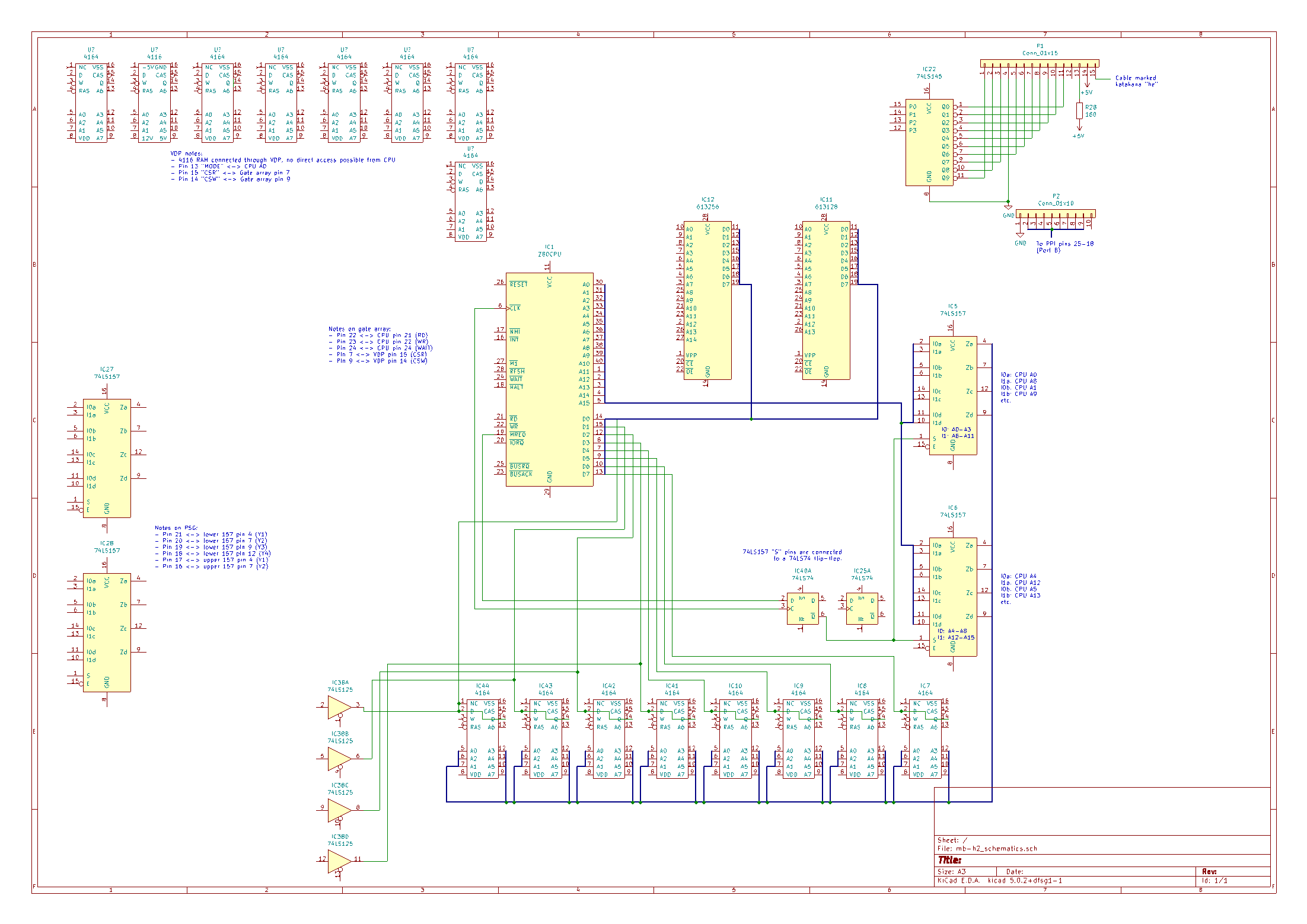
See also Hitachi MB-H2 board pics / more partial “schematics”.
I recently got hold of a Hitachi MB H2 that wouldn’t work. Attaching a composite cable, I’d just see a black screen with some faint colored vertical bars. I probed around the computer with an oscilloscope and found that the computer actually appears to execute code in the first few microseconds or milliseconds after powering it on (or resetting). There didn’t appear to be any bad connections.
I saw some very pronounced unusual voltages on the data bus; judging by the color intensity on the oscilloscope screen I got 33% 0V, 33% about 1-2 V, 33% 5V. The 1-2 V bar could just be everything attached being in a “don’t care”/”high impedance” state, so I proceeded to look for some schematics on the internets. But there were none as far as I can tell! (Anyway, it seems normal to have some not-one-but-not-quite-zero-either activity on this computer as I found out later.)
Having no prior MSX experience, I proceeded to trace out a lot of the connections from the CPU to the other chips. It turned out that most data lines are directly connected to the CPU, implying that most of the chips should have some kind of “don’t care”/”high impedance” state. From the tracing I did I managed to create some partial schematics, until I found I was wise enough to figure some stuff out.
So what’s wrong with my MSX?
There is one thing that seemed very wrong to me on my MSX, I had no activity on the Z80’s IOREQ pin. I also never had activity on the VDP’s pins that interface with the CPU. So I set a rising edge trigger on the Z80’s IOREQ pin and pressed the reset button and saw that there were a couple very early IOREQ signals, suggesting that the computer works normally for at least a while.
A Z80 starts executing from address #0, and the code at this address will have to be on ROM. This machine has 32 KB + 16 KB of ROM, and 64 KB of RAM. A Z80 can only address 64 KB, so we will have to have some kind of mechanism to switch between ROM and RAM. I am not entirely sure how this works on the MSX, but to me it just seemed likely that the early boot code would perhaps copy the ROM contents to RAM and then execute code from there. And if the RAM is defective somehow we’ll be in a bit of a situation… (Even if that isn’t correct, broken RAM should/could/might cause things to go haywire early in the boot process.)
So I suspected the (non-socketed) 4164 RAM is probably broken (I think this is a very common defect for early computers), and set up a small circuit to help me test that theory.
RAM can break in a number of ways, some RAM chips get hot, some pull the data pin to 0 or perhaps 1, and some are perpetually high-impedance, i.e. they do not affect the voltage of the data pin at all. (None of the RAM chips were hot in my case. The video chip is very hot, but the datasheet mentioned something about 70 degrees Celsius so that’s probably fine.)
Unfortunately my oscilloscope only has two inputs. However, to verify if a RAM chip actually does something when somebody reads from it, we may need more, depending on the RAM chip in question of course. Here are some screenshots from the datasheet (TMS4164-datasheet-texas-instruments.pdf):
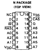
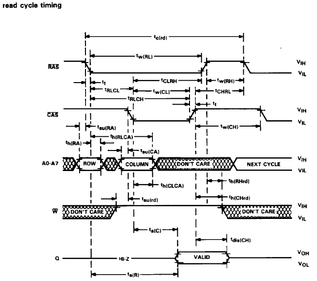
In the read sequence, we see that \CAS (usually high) is low and \W (usually “don’t care”) is high, and after a short moment we see either a low or a high on Q (normally “high impedance”).
So with just two oscilloscope inputs we don’t get very far, we’d need three (for \W, \CAS and Q). However, with a very simple circuit we can get by with two inputs.
All we need is a NOT gate and an AND gate. Then we can combine \W and \CAS and produce H if and only if (\W is high and \CAS is (not high)). So we wire things like this:
       |----|
       |    |--\CAS------NOT----|
--\W-- |    |--Q--probe         AND--probe
|      |4164|                   |
|      |----|                   |
|-------------------------------|
All you need is a breadboard, 74LS04 and a 74LS08 chip. Here’s a picture of the setup:

So let’s have a look at the resulting oscilloscope captures to see if we can find anything interesting. In the captures, the output of the AND gate is in yellow, and the output Q (which is shorted to D on this computer) is blue. Maybe take a look and try to find the problem. The answer is right below the last image so, spoiler warning. ;)


Highlight (and possibly copy and paste somewhere) the next paragraph to read the answer:
D0. Yellow goes high, but blue doesn’t budge at all. We’re trying to read from this chip but the chip isn’t outputting anything!
I piggy-backed (and made sure this particular problem went away) and replaced the suspect chip, but unfortunately it appears that that isn’t all that is wrong with this computer. :/ (If you see this text instead of a link to additional blog posts, that means that I haven’t figured out the problem yet, or haven’t gotten around to creating a write-up for it yet.)
In fact this may have been the only thing wrong with the computer. Piggy-backing unfortunately didn’t work, but after soldering things eventually worked out. I also replaced another RAM chip that seemed like it was misbehaving (More two-channel oscilloscope-based RAM testing) because I was already desoldering, so that could have been part of it too.