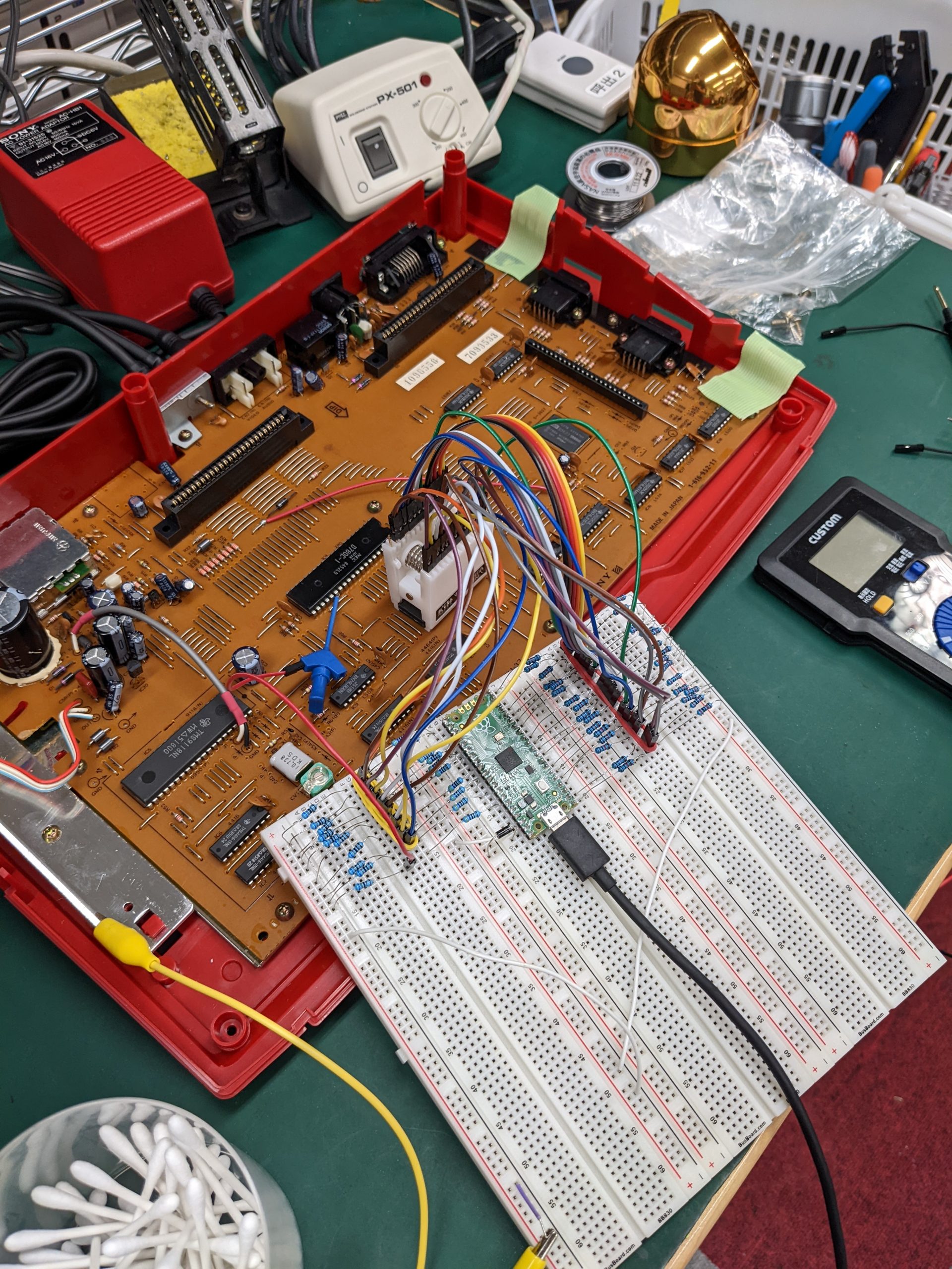
git clone https://github.com/Panda381/PicoVGA
cd PicoVGA/vga_matrixrain
program.uf2 already exists in this directory, you can copy that to your Pico and it will work.
Let’s try to recompile it though:
.../PicoVGA/vga_matrixrain$ makeNothing happens but program.uf2 gets deleted. Great.
Let’s try this instead:
.../PicoVGA/vga_matrixrain$ make program.uf2Output:
ASM ../_boot2/boot2_w25q080_bin.S
Assembler messages:
Fatal error: can't create build/boot2_w25q080_bin.o: No such file or directory
make: *** [../Makefile.inc:469: build/boot2_w25q080_bin.o] Error 1
Let’s create the ‘build’ subdirectory and try again.
.../PicoVGA/vga_matrixrain$ mkdir build

ASM ../_boot2/boot2_w25q080_bin.S
ASM ../_sdk/bit_ops_aeabi.S
ASM ../_sdk/crt0.S
ASM ../_sdk/divider.S
ASM ../_sdk/divider0.S
ASM ../_sdk/double_aeabi.S
ASM ../_sdk/double_v1_rom_shim.S
ASM ../_sdk/float_aeabi.S
ASM ../_sdk/float_v1_rom_shim.S
ASM ../_sdk/irq_handler_chain.S
ASM ../_sdk/mem_ops_aeabi.S
ASM ../_sdk/pico_int64_ops_aeabi.S
ASM ../_picovga/render/vga_atext.S
ASM ../_picovga/render/vga_attrib8.S
ASM ../_picovga/render/vga_color.S
ASM ../_picovga/render/vga_ctext.S
ASM ../_picovga/render/vga_dtext.S
ASM ../_picovga/render/vga_fastsprite.S
ASM ../_picovga/render/vga_ftext.S
ASM ../_picovga/render/vga_graph1.S
ASM ../_picovga/render/vga_graph2.S
ASM ../_picovga/render/vga_graph4.S
ASM ../_picovga/render/vga_graph8.S
ASM ../_picovga/render/vga_graph8mat.S
ASM ../_picovga/render/vga_graph8persp.S
ASM ../_picovga/render/vga_gtext.S
ASM ../_picovga/render/vga_level.S
ASM ../_picovga/render/vga_levelgrad.S
ASM ../_picovga/render/vga_mtext.S
ASM ../_picovga/render/vga_oscil.S
ASM ../_picovga/render/vga_oscline.S
ASM ../_picovga/render/vga_persp.S
ASM ../_picovga/render/vga_persp2.S
ASM ../_picovga/render/vga_plane2.S
ASM ../_picovga/render/vga_progress.S
ASM ../_picovga/render/vga_sprite.S
ASM ../_picovga/render/vga_tile.S
ASM ../_picovga/render/vga_tile2.S
ASM ../_picovga/render/vga_tilepersp.S
ASM ../_picovga/render/vga_tilepersp15.S
ASM ../_picovga/render/vga_tilepersp2.S
ASM ../_picovga/render/vga_tilepersp3.S
ASM ../_picovga/render/vga_tilepersp4.S
ASM ../_picovga/vga_blitkey.S
ASM ../_picovga/vga_render.S
CC ../_sdk/adc.c
CC ../_sdk/binary_info.c
CC ../_sdk/bootrom.c
CC ../_sdk/claim.c
CC ../_sdk/clocks.c
CC ../_sdk/critical_section.c
CC ../_sdk/datetime.c
CC ../_sdk/dma.c
CC ../_sdk/double_init_rom.c
CC ../_sdk/double_math.c
CC ../_sdk/flash.c
CC ../_sdk/float_init_rom.c
CC ../_sdk/float_math.c
CC ../_sdk/gpio.c
CC ../_sdk/i2c.c
CC ../_sdk/interp.c
CC ../_sdk/irq.c
CC ../_sdk/lock_core.c
CC ../_sdk/mem_ops.c
CC ../_sdk/multicore.c
CC ../_sdk/mutex.c
CC ../_sdk/pheap.c
CC ../_sdk/pico_malloc.c
CC ../_sdk/pio.c
CC ../_sdk/platform.c
CC ../_sdk/pll.c
CC ../_sdk/printf.c
CC ../_sdk/queue.c
CC ../_sdk/rp2040_usb_device_enumeration.c
CC ../_sdk/rtc.c
CC ../_sdk/runtime.c
CC ../_sdk/sem.c
CC ../_sdk/spi.c
CC ../_sdk/stdio.c
CC ../_sdk/stdio_semihosting.c
CC ../_sdk/stdio_uart.c
CC ../_sdk/stdio_usb.c
CC ../_sdk/stdio_usb_descriptors.c
CC ../_sdk/stdlib.c
CC ../_sdk/sync.c
CC ../_sdk/time.c
CC ../_sdk/timeout_helper.c
CC ../_sdk/timer.c
CC ../_sdk/uart.c
CC ../_sdk/unique_id.c
CC ../_sdk/vreg.c
CC ../_sdk/watchdog.c
CC ../_sdk/xosc.c
CC ../_tinyusb/bsp/raspberry_pi_pico/board_raspberry_pi_pico.c
CC ../_tinyusb/class/audio/audio_device.c
CC ../_tinyusb/class/bth/bth_device.c
CC ../_tinyusb/class/cdc/cdc_device.c
CC ../_tinyusb/class/cdc/cdc_host.c
CC ../_tinyusb/class/cdc/cdc_rndis_host.c
CC ../_tinyusb/class/dfu/dfu_rt_device.c
CC ../_tinyusb/class/hid/hid_device.c
CC ../_tinyusb/class/hid/hid_host.c
CC ../_tinyusb/class/midi/midi_device.c
CC ../_tinyusb/class/msc/msc_device.c
CC ../_tinyusb/class/msc/msc_host.c
CC ../_tinyusb/class/net/net_device.c
CC ../_tinyusb/class/usbtmc/usbtmc_device.c
CC ../_tinyusb/class/vendor/vendor_device.c
CC ../_tinyusb/class/vendor/vendor_host.c
CC ../_tinyusb/common/tusb_fifo.c
CC ../_tinyusb/device/usbd.c
CC ../_tinyusb/device/usbd_control.c
CC ../_tinyusb/host/ehci/ehci.c
CC ../_tinyusb/host/ohci/ohci.c
CC ../_tinyusb/host/hub.c
CC ../_tinyusb/host/usbh.c
CC ../_tinyusb/host/usbh_control.c
CC ../_tinyusb/portable/raspberrypi/rp2040/dcd_rp2040.c
CC ../_tinyusb/portable/raspberrypi/rp2040/hcd_rp2040.c
CC ../_tinyusb/portable/raspberrypi/rp2040/rp2040_usb.c
CC ../_tinyusb/tusb.c
C++ src/main.cpp
In file included from src/main.cpp:8:0:
src/include.h:13:10: fatal error: ../vga.pio.h: No such file or directory
 #include "../vga.pio.h"  // VGA PIO compilation
          ^~~~~~~~~~~~~~
compilation terminated.
make: *** [../Makefile.inc:458: build/main.o] Error 1
Where do we get vga.pio.h? It’s nowhere in the directory.
Let’s take a look at vga_matrixrain/c.bat:
...
..\_exe\pioasm.exe -o c-sdk ..\_picovga\vga.pio vga.pio.h
...
Hey! pioasm. The repository contains an exe file for this. Is it part of the Pico SDK?
Try:
.../PicoVGA/vga_matrixrain$ locate pioasmI found it in one of my SDK-related directories. Cool. Let’s try it.
.../picoprobe/build/pioasm/pioasm -o c-sdk ../_picovga/vga.pio vga.pio.h
../_picovga/vga.pio:1.1: invalid character:
    1 |
      | ^
../_picovga/vga.pio:13.1: invalid character:
   13 |
      | ^
../_picovga/vga.pio:14.13: invalid character:
   14 | .program vga
      |             ^
../_picovga/vga.pio:17.1: invalid character:
   17 |
      | ^
../_picovga/vga.pio:19.1: invalid character:
   19 |
      | ^
../_picovga/vga.pio:20.13: invalid character:
   20 | public sync:
      |             ^
../_picovga/vga.pio:22.11: invalid character:
   22 | sync_loop:
      |           ^

too many errors; aborting.
One look at hexdump -C ../_picovga/vga.pio | less, we see CRLF line endings. Let’s get rid of them and try again:
tr -d '\015' < ../_picovga/vga.pio > ../_picovga/vga.pio.unix
mv ../_picovga/vga.pio > ../_picovga/vga.pio.windows
mv ../_picovga/vga.pio.unix ../_picovga/vga.pio

.../picoprobe/build/pioasm/pioasm -o c-sdk ../_picovga/vga.pio vga.pio.h # no errors!
Success! Let’s try compiling a little more.
.../PicoVGA/vga_matrixrain$ make program.uf2
C++ src/main.cpp
C++ ../_picovga/vga.cpp
C++ ../_picovga/vga_layer.cpp
C++ ../_picovga/vga_pal.cpp
C++ ../_picovga/vga_screen.cpp
C++ ../_picovga/vga_util.cpp
C++ ../_picovga/vga_vmode.cpp
C++ ../_picovga/util/canvas.cpp
C++ ../_picovga/util/mat2d.cpp
C++ ../_picovga/util/overclock.cpp
C++ ../_picovga/util/print.cpp
C++ ../_picovga/util/rand.cpp
C++ ../_picovga/util/pwmsnd.cpp
C++ ../_picovga/font/font_bold_8x8.cpp
C++ ../_picovga/font/font_bold_8x14.cpp
C++ ../_picovga/font/font_bold_8x16.cpp
C++ ../_picovga/font/font_boldB_8x14.cpp
C++ ../_picovga/font/font_boldB_8x16.cpp
C++ ../_picovga/font/font_game_8x8.cpp
C++ ../_picovga/font/font_ibm_8x8.cpp
C++ ../_picovga/font/font_ibm_8x14.cpp
C++ ../_picovga/font/font_ibm_8x16.cpp
C++ ../_picovga/font/font_ibmtiny_8x8.cpp
C++ ../_picovga/font/font_italic_8x8.cpp
C++ ../_picovga/font/font_thin_8x8.cpp
C++ ../_sdk/new_delete.cpp
ld build/program.elf
uf2 program.uf2
make: execvp: ../_exe/elf2uf2.exe: Permission denied
make: *** [../Makefile.inc:435: program.uf2] Error 127
elf2uf2, I’ve seen that before. Let’s check if that’s in the SDK.
.../PicoVGA/vga_matrixrain$ locate elf2uf2Found it.
.../picoprobe/build/elf2uf2/elf2uf2Let’s see what exactly needs to be executed here:
make --trace program.uf2
../Makefile.inc:434: update target 'program.uf2' due to: build/program.elf
echo     uf2             program.uf2
uf2 program.uf2
../_exe/elf2uf2.exe build/program.elf program.uf2
make: execvp: ../_exe/elf2uf2.exe: Permission denied
make: *** [../Makefile.inc:435: program.uf2] Error 127
All right, so we just have to do:
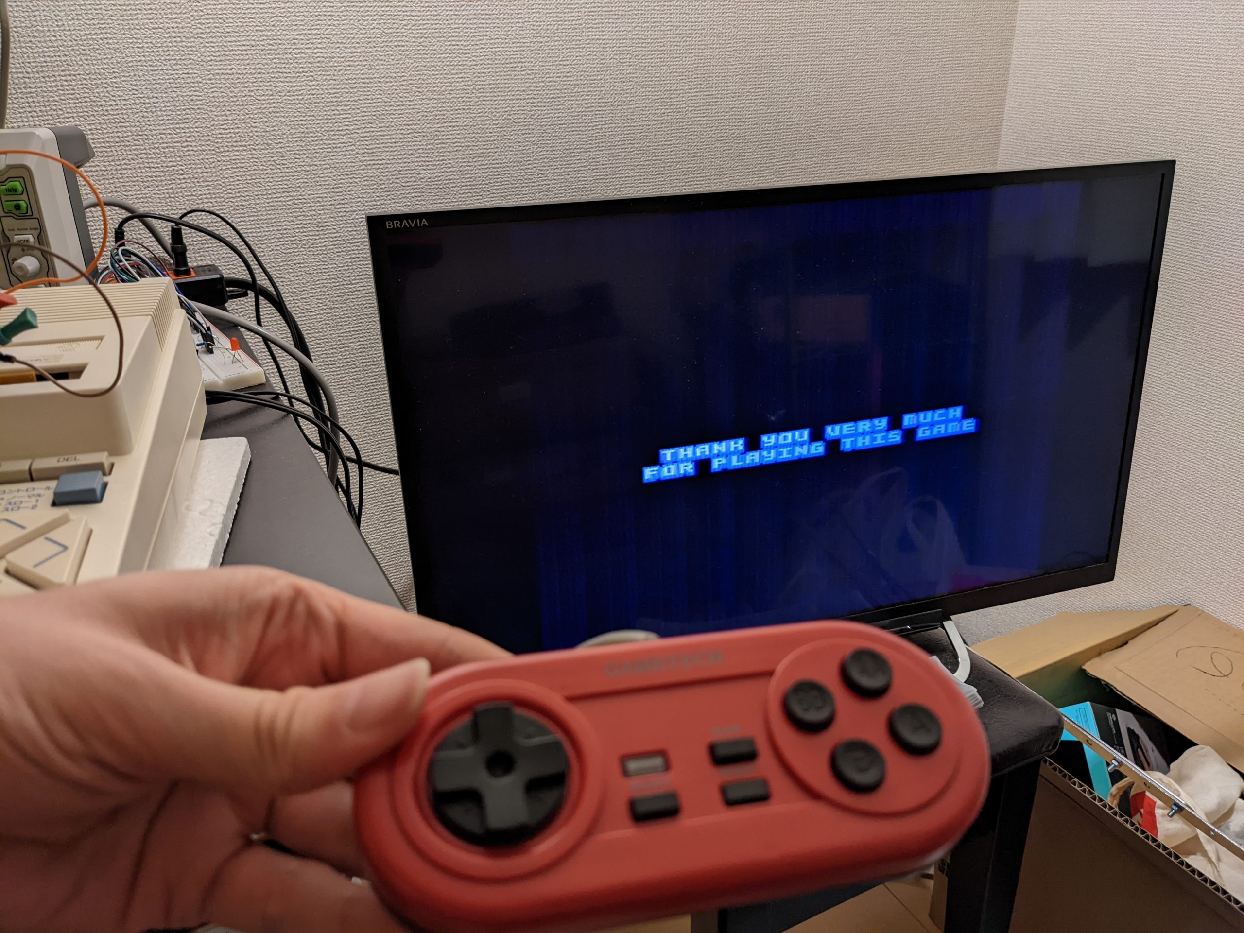
.../PicoVGA/vga_matrixrain$ .../picoprobe/build/elf2uf2/elf2uf2 build/program.elf program.uf2Let’s put that on the Pico and see what happens.
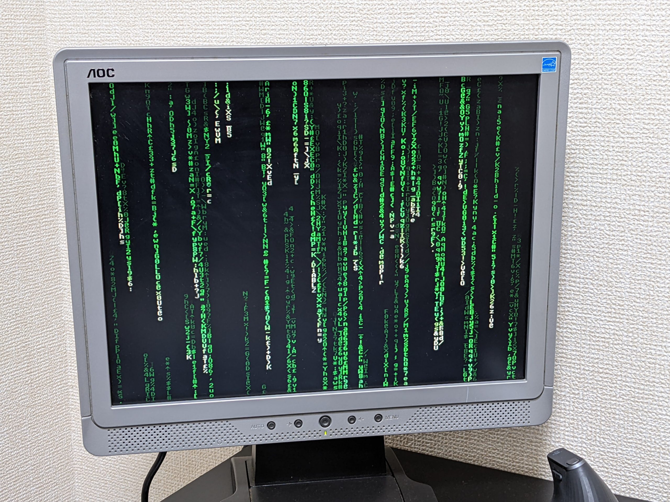

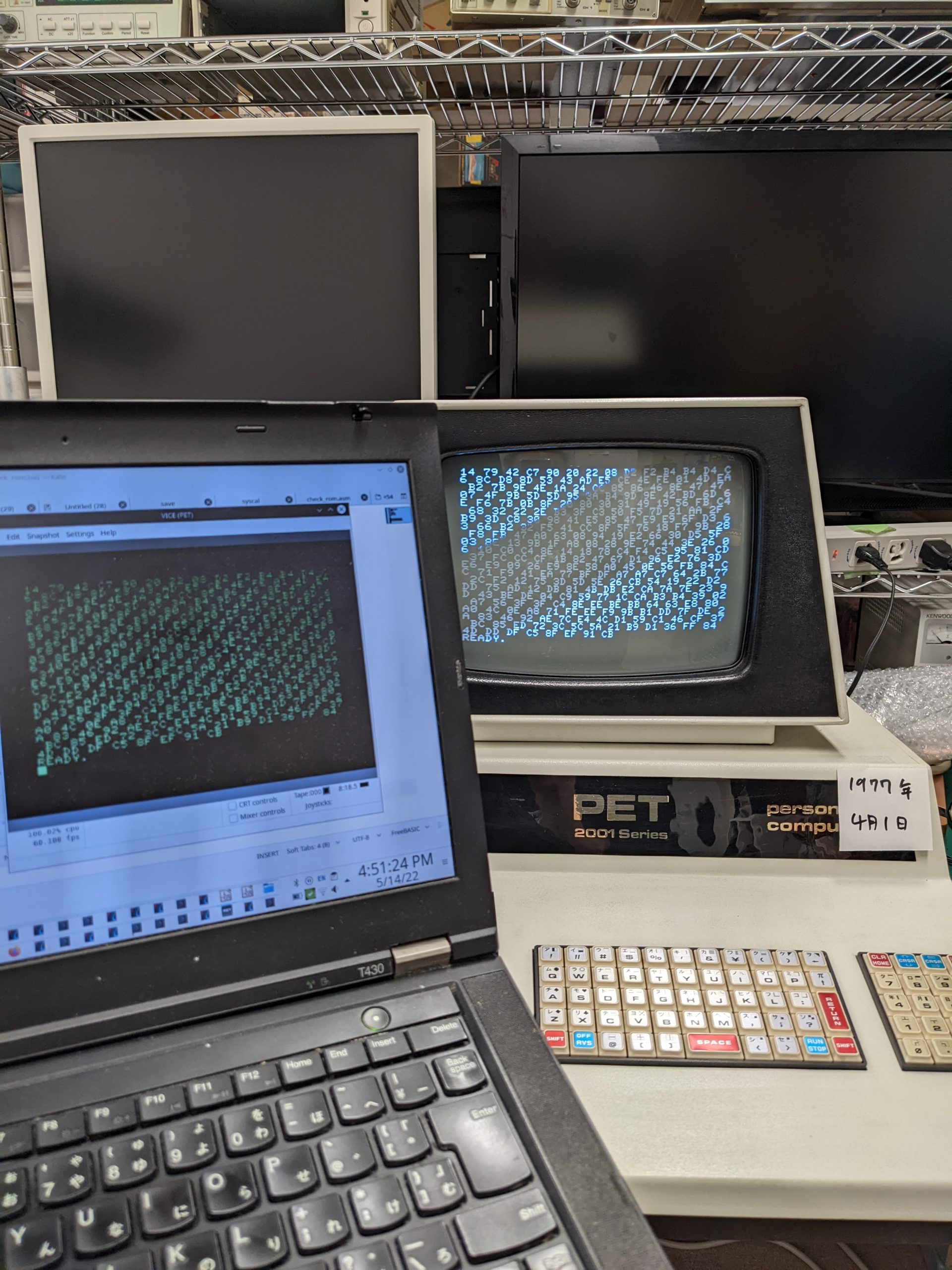
Success!
Edit Makefile.inc like this to get the build system find elf2uf in the correct location:
diff --git a/Makefile.inc b/Makefile.inc
index 3130ab5..03cf706 100644
--- a/Makefile.inc
+++ b/Makefile.inc
@@ -349,7 +349,7 @@ NM = ${COMP}nm
 SZ = ${COMP}size

 # uf2
-UF = ../_exe/elf2uf2.exe
+UF = /path/to/picoprobe/build/elf2uf2/elf2uf2

 ##############################################################################
 # File list


