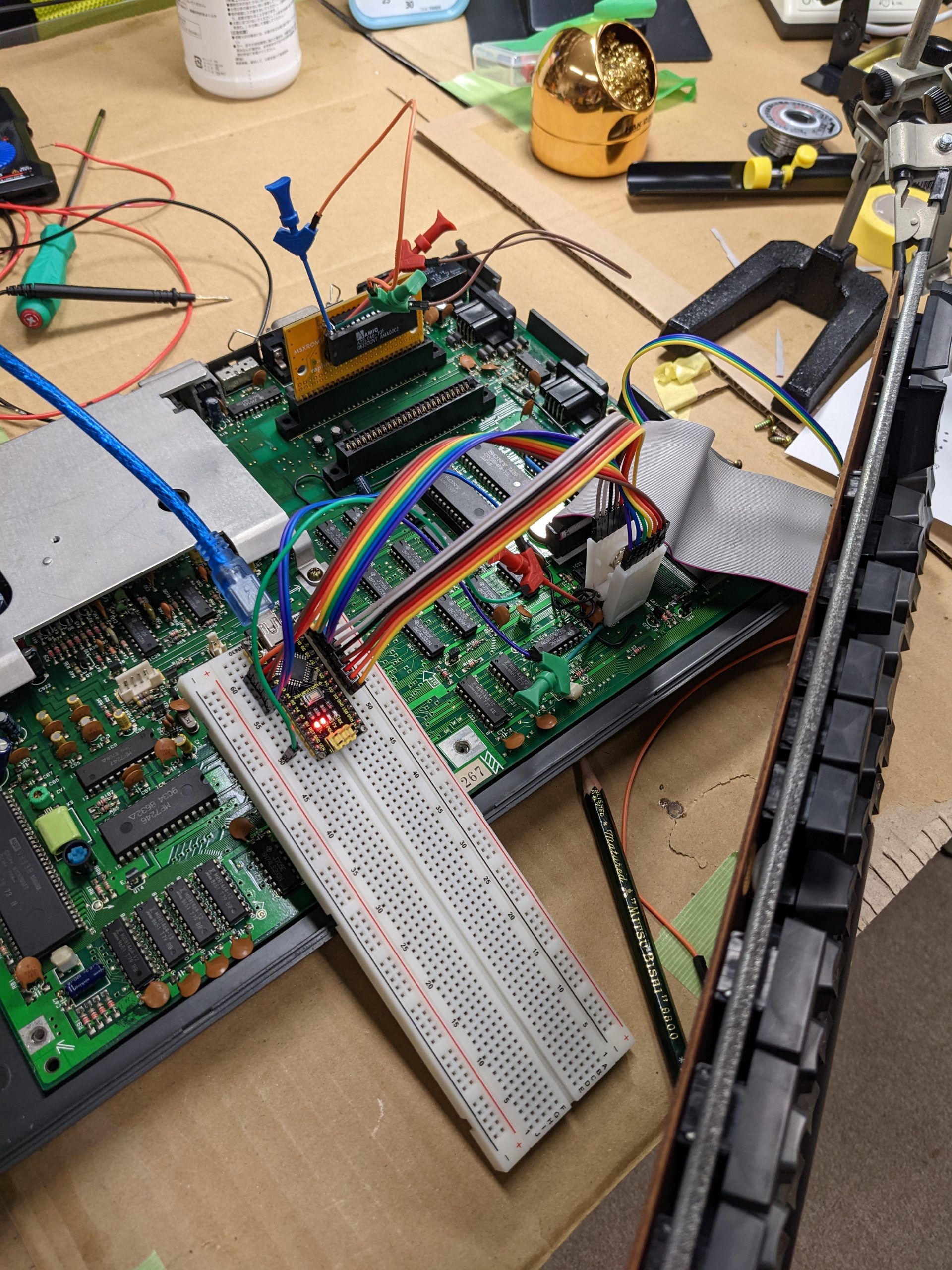
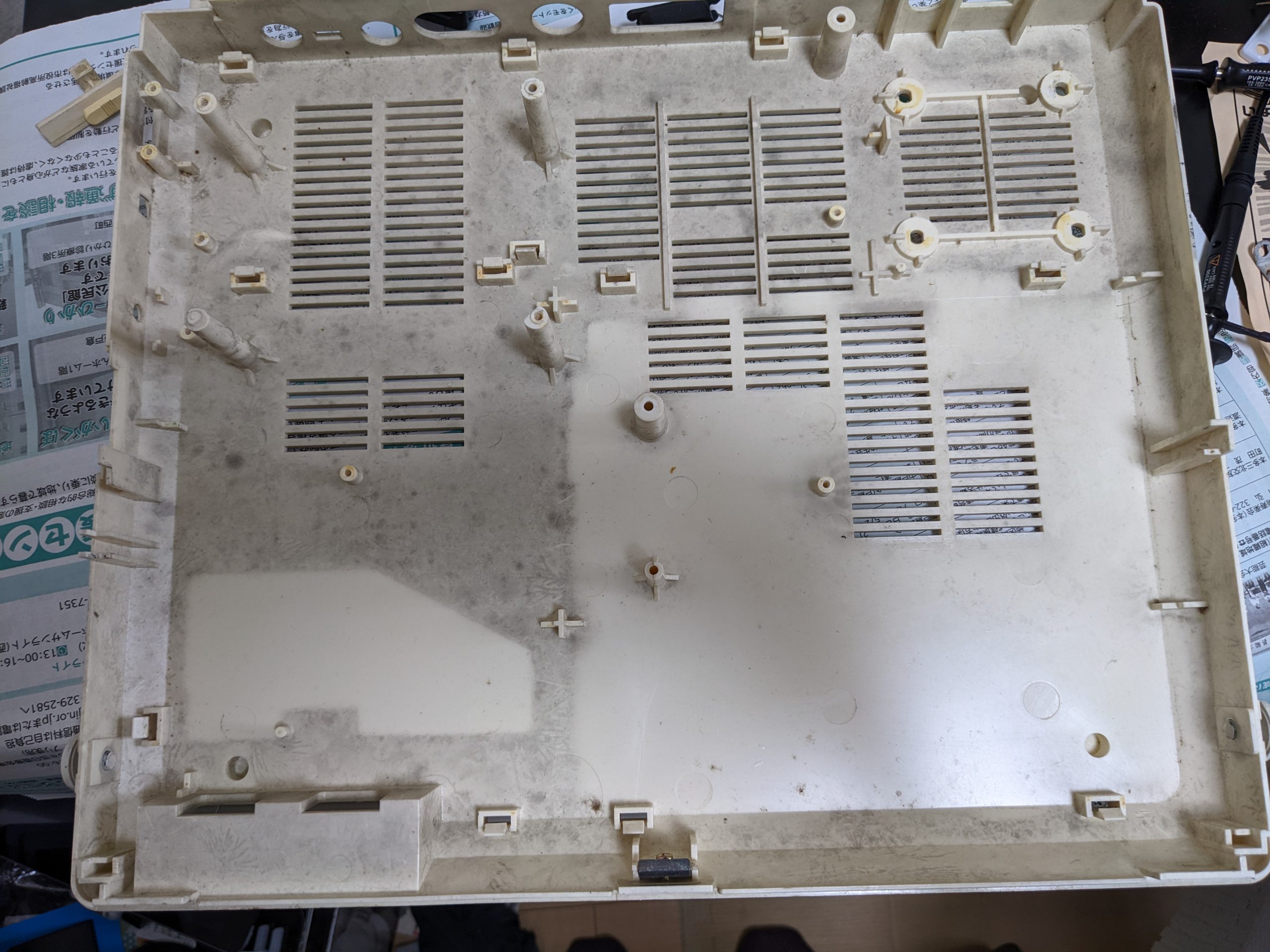
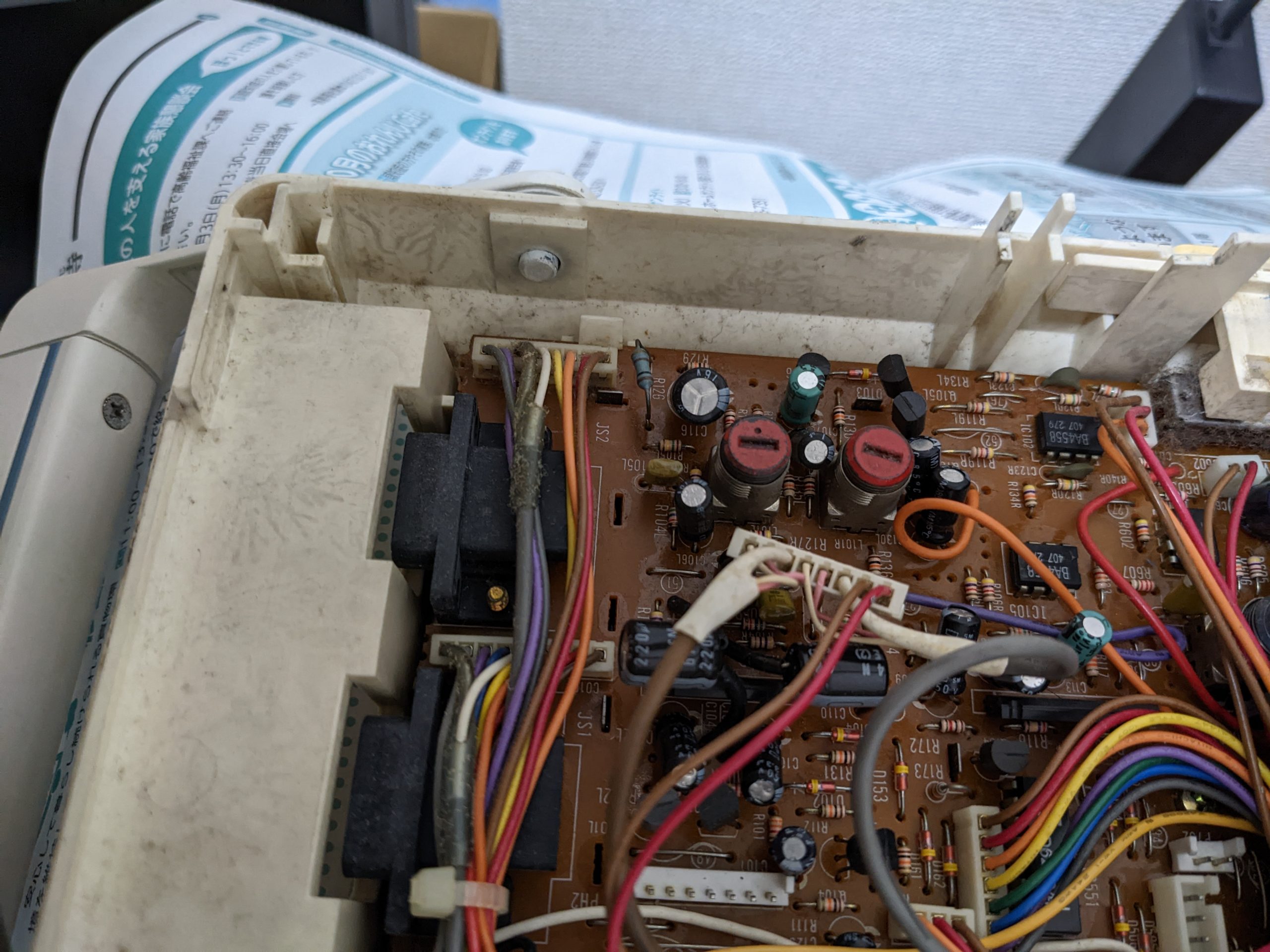
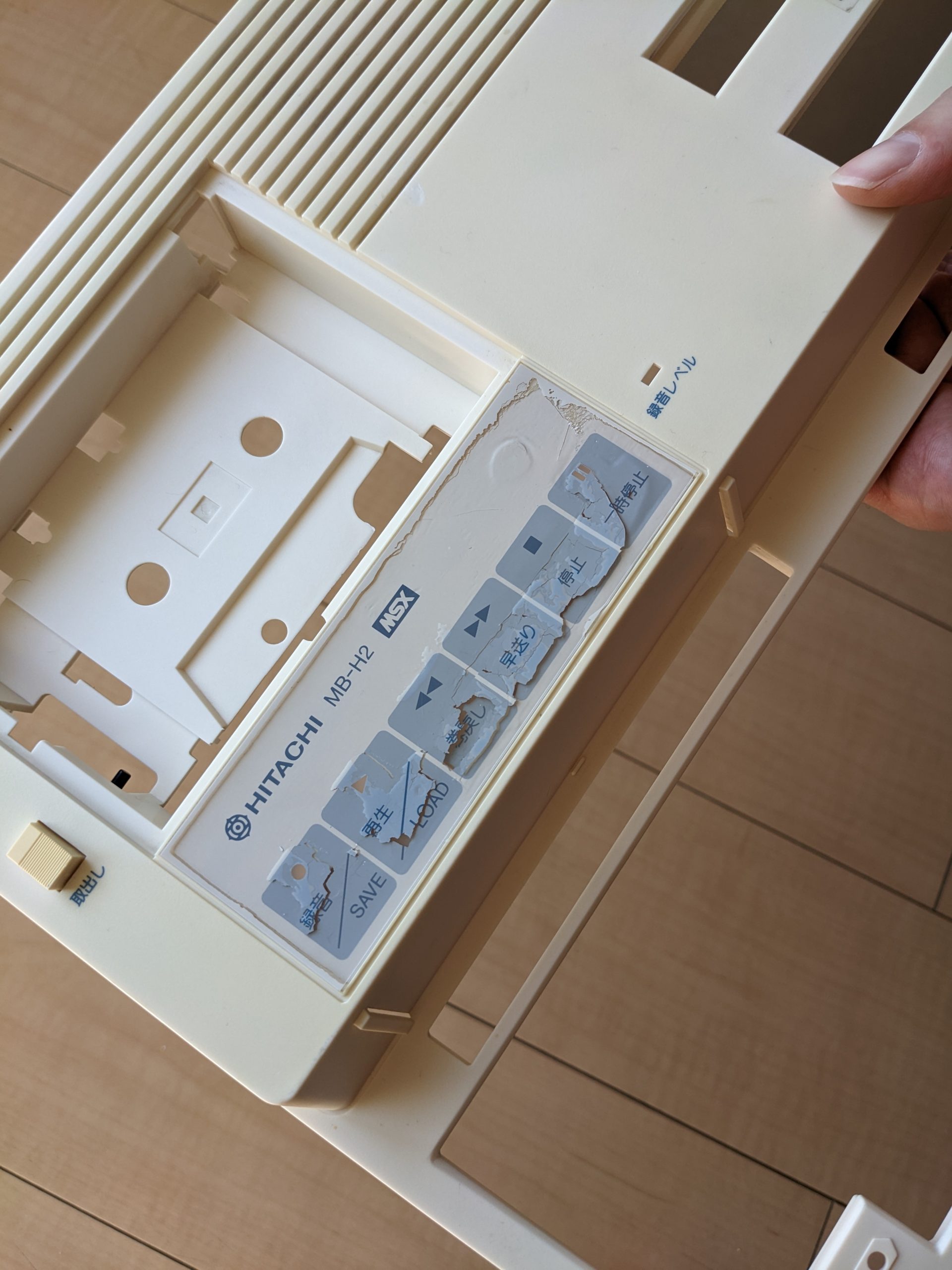
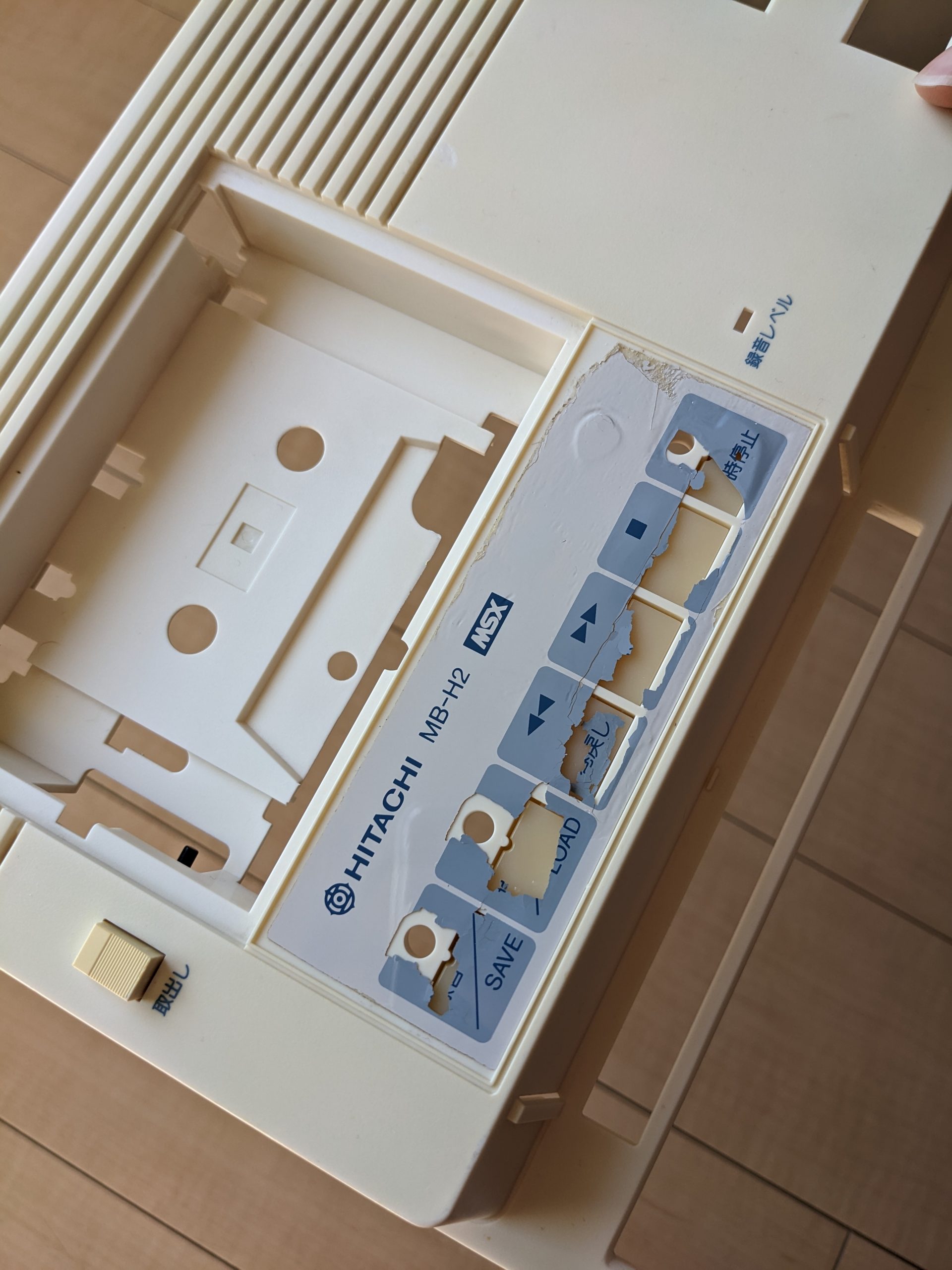
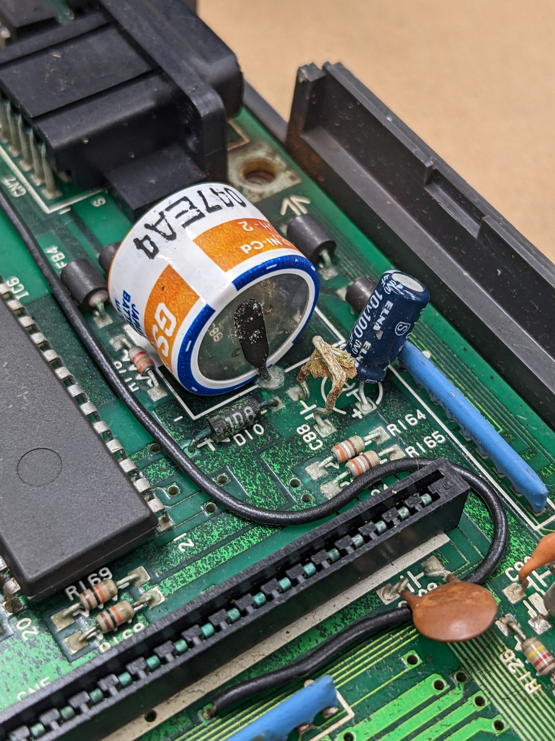
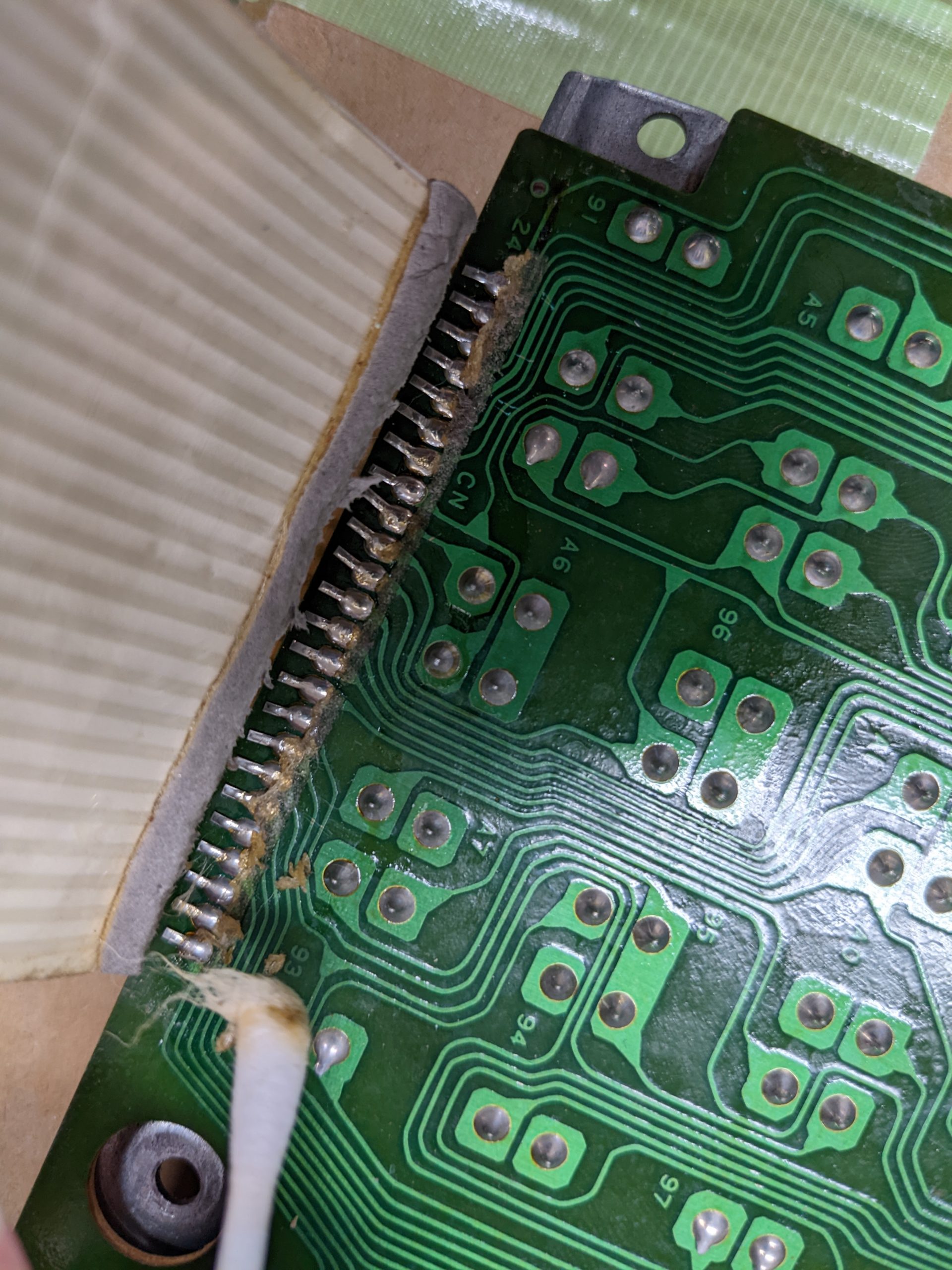
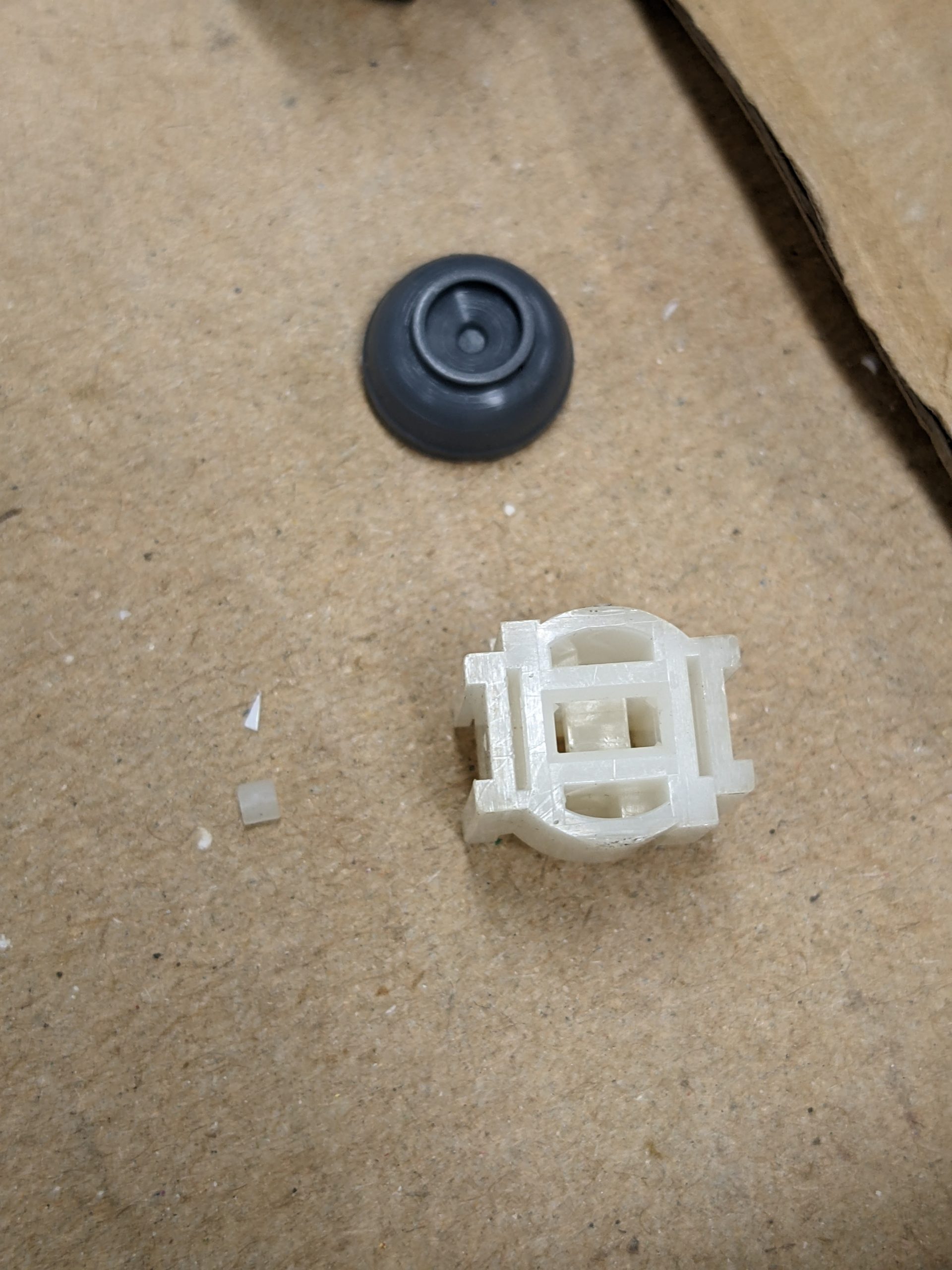
Last year, I bought a faulty Hitachi MB-H2 (MSX) in order to gain electronics and repair experience. Using my oscilloscope and two simple 74-series (NOT and AND) logic ICs, I managed to figure out that one of the RAM chips was faulty. I replaced the RAM chip, but it still wouldn’t work. I did one more slightly less reliable oscilloscope-based test and replaced one more chip, and it still wouldn’t work. How many faults can this machine have? Well it turns out that probably only the first RAM chip was broken in the first place, and I just didn’t solder properly. I thought I had checked my connections, but I guess one was border-line. (I have more soldering experience now.)
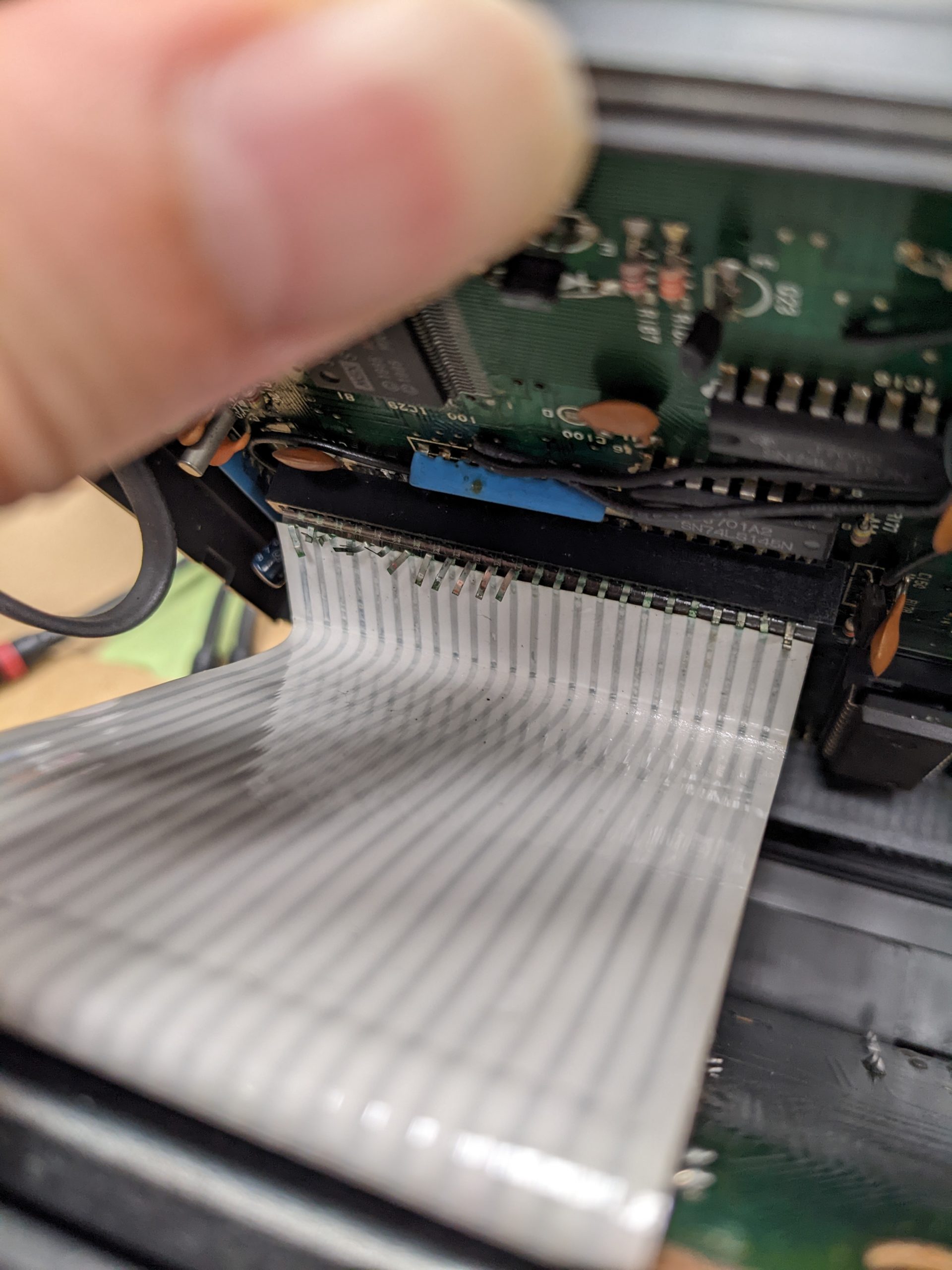
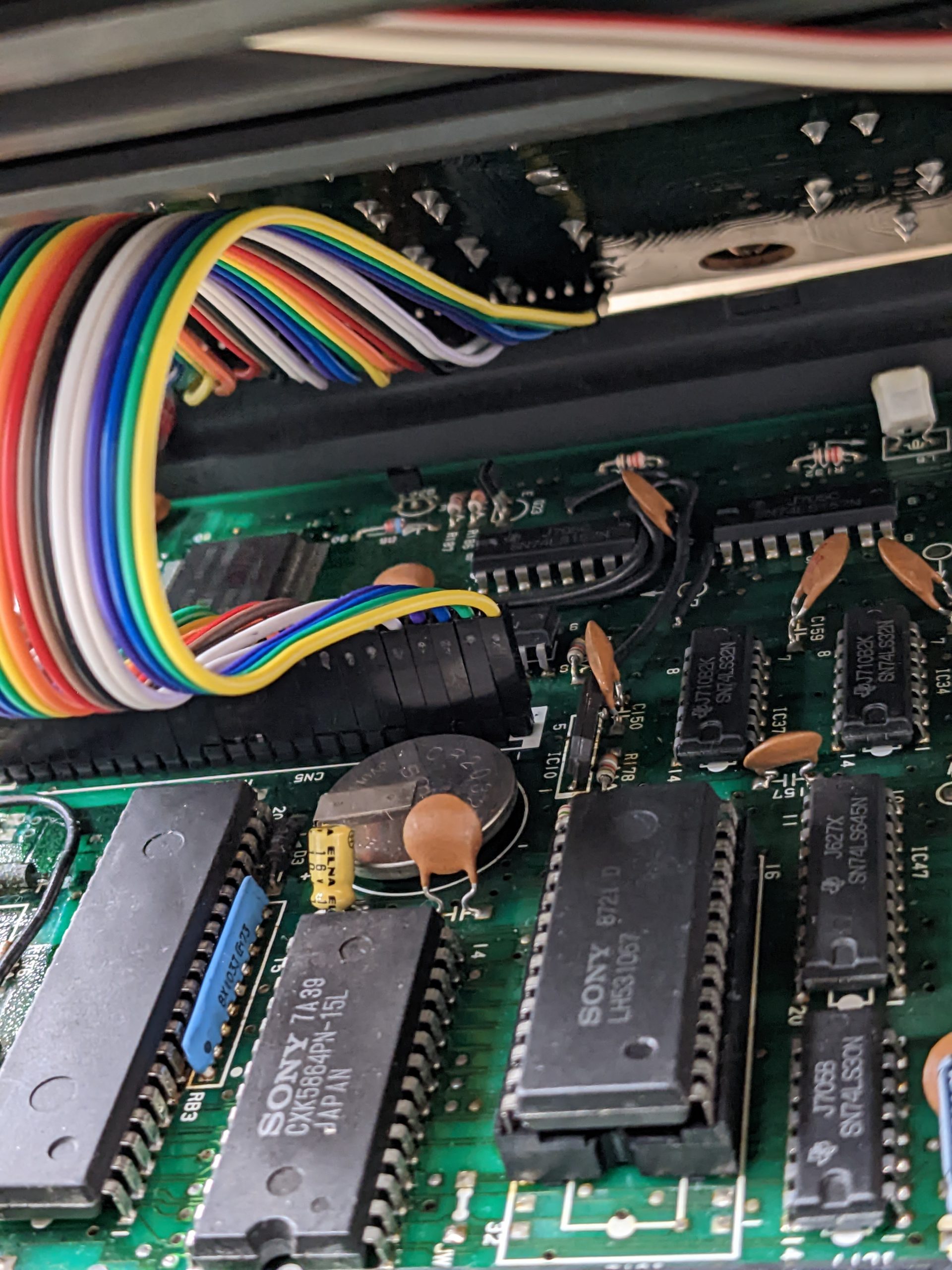
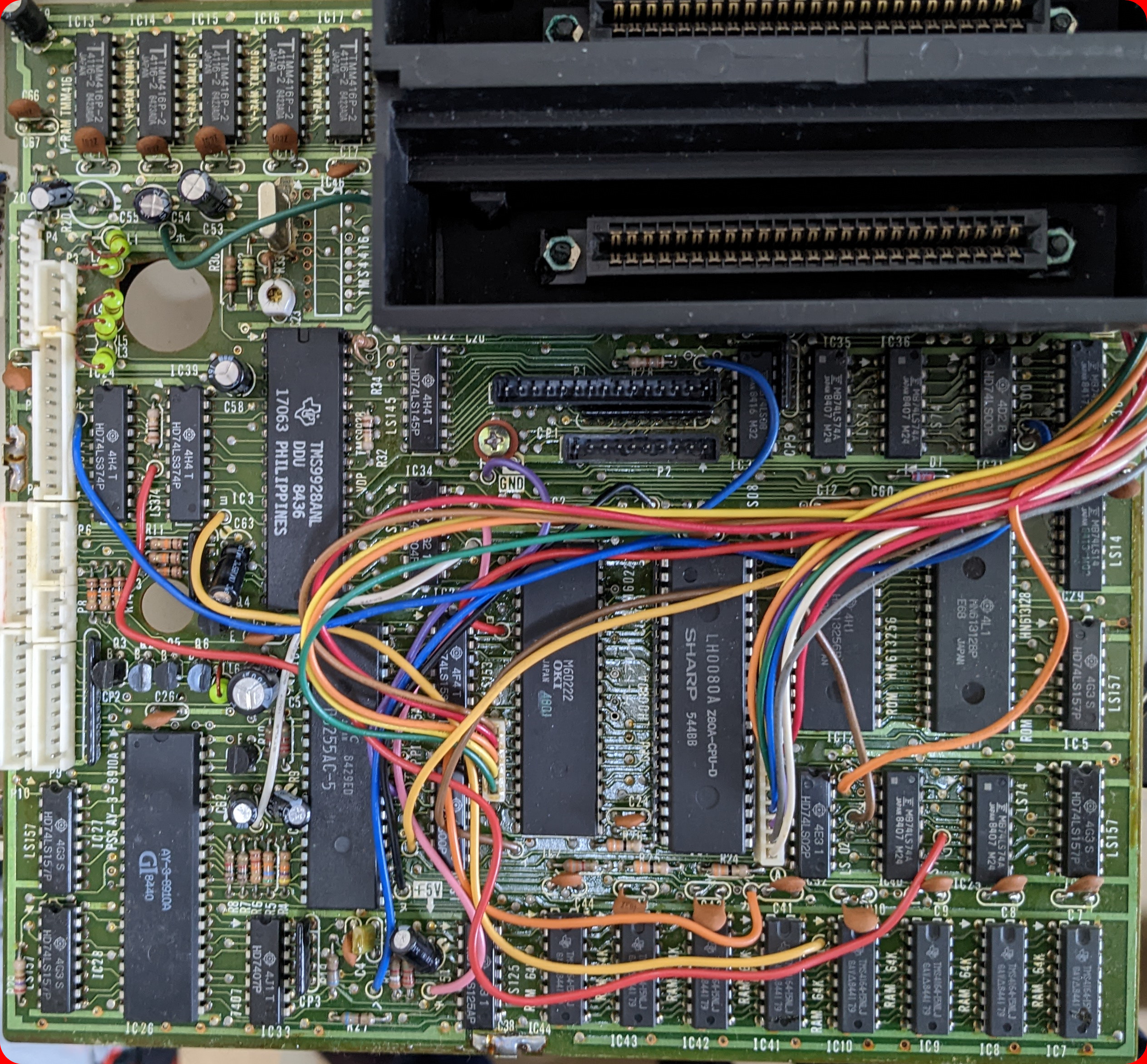
So, suspecting that I had some kind of severe fault, and not having come up with the logic analyzer “idea” yet, and noticing that the CPU was socketed, I decided to take out the CPU and just generate the signals that the CPU would generate myself, using two Raspberry Pi Picos. (Because I needed a lot of pins, not necessarily performance.) One Pico is responsible for the address and control pins, the other for the data pins. As I noticed some time in, Pico 1 should have had the data and control pins, Pico 2 the address pins. Why? Timing matters with the data pins, but for address pins you can be super slow and it’ll be fine. It still worked out in the end.
Pico 1 controls Pico 2 via UART. A host computer (yes, you, Mr. ThinkPad) controls Pico 1 via serial. Then some idiot (yes, me) types in commands into a serial terminal, and Pico 1 does the idiot’s bidding. The following commands are recognized:
- i, for IOREQ input
- o, for IOREQ output
- v, for VRAM manipulation, which I actually couldn’t get to work the way I expected, but it still does something
- r, for RAM reads
- w, for RAM writes (and a simple readback to make sure the RAM stores stuff)
- W, for RAM writes with RAM refresh (and a readback after every refresh). You can specify the amount of writes between refreshes and stuff.
- s, sync UART (flushes out all characters stuck in the UART read buffer)
- 0: ask Pico 2 to set data bus to 0
- u: ask Pico 2 to unset data bus (i.e., to set bus direction from: GPIO_OUT to: GPIO_IN)
So, how does it work? How does the Z80 work? Let’s have a look at the Z80 pinout:
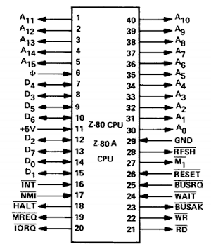
The A pins are the address pins. The D pins are the data pins. So if you want to write 0 to address 0, all those pins will be 0. In addition, RD will be high, and WR will be low, because we are writing. (Yes, 0 means “active” and 1 means “inactive”.) In addition, we are writing to memory, not to IO space. So IORQ is 1 and MREQ is 0. (Also M1 goes from 1 to 0 too, but I don’t remember the details there.) If we instead want to talk to hardware, we need to know the hardware address and set IORQ to 0 instead of MREQ. On the Z80, only A0 to A7 matter for IO addresses. Well, that’s the gist of it.
With a crude thing like this, we can:
- Dump the main ROM and check that the contents are correct
- Check if memory works
- Check if the sound chip works
- Check if the video chip works
- Check if the IO controller works
- We can turn the tape motor on and off
- We can map memory
- Etc.?
- (Provided the connection from CPU to the above peripherals is working)
I was able to check all of the above. Note that in the highly unlikely event that you decide to run any of this on your MSX machine, note that memory mapping is a bit different from machine to machine. (Which is important, otherwise RAM expansions wouldn’t work, right?)
So here are some examples of commands I’d paste into my terminal:
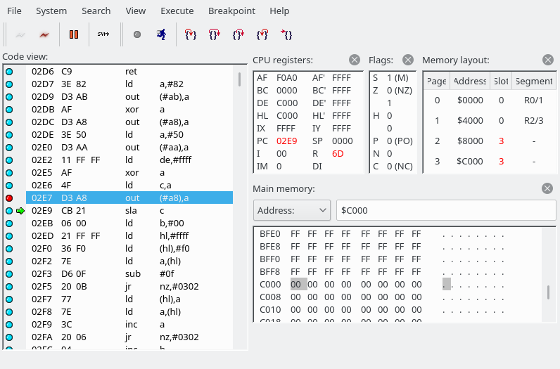
# Turn off tape motor (which is on by default IIRC?), map memory, maybe some other stuff (I got these by running the MB-H2 in openmsx and checking the earliest 'in's and 'out's in openmsx-debugger, also see below screenshot)
# Execute this before executing anything else!
o00ab82o00aa50o00a800o00a850o00a8a0o00a8f0

# Read first 16 bytes of ROM
r0000rr0001rr0002rr0003rr0004rr0005rr0006rr0007rr0008rr0009rr000arr000brr000crr000drr000err000frr0010r

# Read bits 0, 1, 2, 3, 4, 5, 6, 7, 8, 9, 10, 11, 12, 13, 14, and 15 (counting bits from 0) (if you get the right result here you'll know that your connections are good)
r0001rr0002rr0004rr0008rr0010rr0020rr0040rr0080rr0100rr0200rr0400rr0800rr1000rr2000rr4000rr8000r

# Expected result of above command for MB-H2:
sed -n -e '2p' -e '3p' -e '5p' -e '9p' -e '17p' -e '33p' -e '65p' -e '129p' -e '257p' -e '513p' -e '1025p' -e '2049p' -e '4097p' -e '8193p' -e '16385p' 32k_v2.hex
c3
d7
bf
c3
c3
c3
13
06
ee
2a
e5
32
a4
00
e5
head -n 1 16k_v2.hex
41

# Set background colors:
o00990fo009987 # white background
o00990eo009987 # gray
o00990do009987 # magenta
o00990co009987 # dark green
o00990bo009987 # light yellow
o00990ao009987 # dark yellow
o009909o009987 # light red
o009908o009987 # medium red
o009907o009987 # cyan
o009906o009987 # dark red
o009905o009987 # light blue
o009904o009987 # dark blue
o009903o009987 # light green
o009902o009987 # medium green
o009901o009987 # black

# click sound test:
o00ab0fo00ab0eo00ab0fo00ab0eo00ab0fo00ab0e

# VRAM notes (worked partially, but I think you may need to change the video mode to something else in order to get full VRAM access like this? Never really got it to work as expected. IIRC, the values would stick for a bit, and then go back to 0f or something)
# To read from 0000 to ... (address is auto-incremented, so you only have to set it once):
o009900 # set lower byte of address
o009900 # set upper byte of address (bit 7 and 6 are low to indicate that we want to read)
i0098 # read from 0000
i0098 # read from 0001
i0098 # read from 0002
i0098 # read from 0003
...
# bunched into a single line:
o009900o009900i0098i0098i0098i0098
# To write ff to 0000-... (address is auto-incremented, so you only have to set it once):
o009900 # set lower byte of address
o009940 # set upper byte of address (bit 7 is low and bit 6 is high to indicate that we want to write)
o0098ff # set data register to ff to write to 0000
o0098ff # set data register to ff to write to 0001
o0098ff # set data register to ff to write to 0002
o0098ff # set data register to ff to write to 0003
...
# bunched into a single line:
o009900o009940o0098ffo0098ffo0098ff
What’s a good story without pictures?
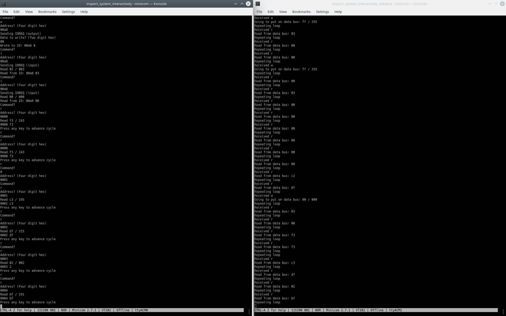

BTW, just one Pico here because I thought it’d be worth something with just a couple bits on the data bus. But yeah, that wasn’t very fun.

sleep 5
send o009900o009980\c
send o009903o009981\c
send o009900o009987\c
sleep 1
send o009901o009987\c
sleep 1
send o009902o009987\c
sleep 1
send o009903o009987\c
sleep 1
send o009904o009987\c
sleep 1
send o009905o009987\c
sleep 1
send o009906o009987\c
sleep 1
send o009907o009987\c
sleep 1
send o009908o009987\c
sleep 1
send o009909o009987\c
sleep 1
send o00990ao009987\c
sleep 1
send o00990bo009987\c
sleep 1
send o00990co009987\c
sleep 1
send o00990do009987\c
sleep 1
send o00990eo009987\c
sleep 1
send o00990fo009987\c
The code
Danger: do not submit code to code beauty contests.
The code consists of two separate projects, in CMake terms. One is for Pico 1, the other is for Pico 2. First of all the CMakeLists.txt files are as follows:
Pico 1 (create a directory called e.g. inspect_system_interactively and in there, create a file called CMakeLists.txt with the following contents):
cmake_minimum_required(VERSION 3.12)

# Pull in SDK (must be before project)
include(pico_sdk_import.cmake)

project(pico_examples C CXX ASM)
set(CMAKE_C_STANDARD 11)
set(CMAKE_CXX_STANDARD 17)

if (PICO_SDK_VERSION_STRING VERSION_LESS "1.3.0")
    message(FATAL_ERROR "Raspberry Pi Pico SDK version 1.3.0 (or later) required. Your version is ${PICO_SDK_VERSION_STRING}")
endif()

set(PICO_EXAMPLES_PATH ${PROJECT_SOURCE_DIR})

# Initialize the SDK
pico_sdk_init()

include(example_auto_set_url.cmake)

add_compile_options(-Wall -Wextra
        -Wno-format          # int != int32_t as far as the compiler is concerned because gcc has int32_t as long int
        -Wno-unused-function # we have some for the docs that aren't called
        -Wno-maybe-uninitialized
        -O3
        )

add_executable(inspect_system_interactively
        inspect_system_interactively.c
        )

# pull in common dependencies
target_link_libraries(inspect_system_interactively pico_stdlib)

# enable usb output, disable uart output
pico_enable_stdio_usb(inspect_system_interactively 1)
pico_enable_stdio_uart(inspect_system_interactively 0)

# create map/bin/hex file etc.
pico_add_extra_outputs(inspect_system_interactively)

# add url via pico_set_program_url
example_auto_set_url(inspect_system_interactively)
Pico 2 (my directory name is inspect_system_interactively_databus):
cmake_minimum_required(VERSION 3.12)

# Pull in SDK (must be before project)
include(pico_sdk_import.cmake)

project(pico_examples C CXX ASM)
set(CMAKE_C_STANDARD 11)
set(CMAKE_CXX_STANDARD 17)

if (PICO_SDK_VERSION_STRING VERSION_LESS "1.3.0")
    message(FATAL_ERROR "Raspberry Pi Pico SDK version 1.3.0 (or later) required. Your version is ${PICO_SDK_VERSION_STRING}")
endif()

set(PICO_EXAMPLES_PATH ${PROJECT_SOURCE_DIR})

# Initialize the SDK
pico_sdk_init()

include(example_auto_set_url.cmake)

add_compile_options(-Wall -Wextra
        -Wno-format          # int != int32_t as far as the compiler is concerned because gcc has int32_t as long int
        -Wno-unused-function # we have some for the docs that aren't called
        -Wno-maybe-uninitialized
        -O3
        )

add_executable(inspect_system_interactively_databus
        inspect_system_interactively_databus.c
        )

# pull in common dependencies
target_link_libraries(inspect_system_interactively_databus pico_stdlib)

# enable usb output, disable uart output
pico_enable_stdio_usb(inspect_system_interactively_databus 1)
pico_enable_stdio_uart(inspect_system_interactively_databus 0)

# create map/bin/hex file etc.
pico_add_extra_outputs(inspect_system_interactively_databus)

# add url via pico_set_program_url
example_auto_set_url(inspect_system_interactively_databus)
You can get the referenced pico_sdk_import.cmake and example_auto_set_url.cmake files from the pico-examples repository (https://github.com/raspberrypi/pico-examples.git).
Next, you need to place the C files into the corresponding directories. Then you just need to execute two commands, “cmake .” followed by “make”, in both directories.
inspect_system_interactively/inspect_system_interactively.c:
#include <stdio.h>
#include "pico/stdlib.h"

#define A11          0
#define A12          1
#define A13          2
#define A14          3
#define A15          4

#define A10         28
#define A9          27
#define A8          26
#define A7          22
#define A6          21
#define A5          20
#define A4          19
#define A3          18
#define A2          17
#define A1          15
#define A0          14

#define MREQ        16 /* active-low */
#define M1          13 /* active-low, we should probably set this and un-set when we're done reading */
#define RFSH        12 /* active-low and we won't be refreshing at all; tie to +5; could also feed inverted MREQ_RD if things don't work otherwise <-- chose to do this */
#define RD           5 /* active-low */
#define WR           6 /* active-low */
#define IOREQ        7 /* active-low */
/* #define HALT        active-low but shouldn't be a problem to keep this floating */

#define UART1_TX     8
#define UART1_RX     9
// #define BAUD    345600
#define BAUD    460800

#define READ_BACK_SIGNAL 10
#define READ_BACK_SIGNAL_ACK 11

#define HIGH         1
#define LOW          0

#ifndef PICO_DEFAULT_LED_PIN
#error blink requires a board with a regular LED
#endif

#define STATUS_LED PICO_DEFAULT_LED_PIN
// #define STATUS_LED 15

#define BUS_SIZE 16

// #define SLOW_PERF 1

const unsigned int a_bus[BUS_SIZE] = {
  A0, A1, A2, A3, A4, A5, A6, A7, A8, A9, A10, A11, A12, A13, A14, A15
};

#define println printf
// #define printf(...) ;

inline void nop(void) {
    __asm__ __volatile__("nop\t\n");
}

void setup() {
    gpio_init(A0);
    gpio_init(A1);
    gpio_init(A2);
    gpio_init(A3);
    gpio_init(A4);
    gpio_init(A5);
    gpio_init(A6);
    gpio_init(A7);
    gpio_init(A8);
    gpio_init(A9);
    gpio_init(A10);
    gpio_init(A11);
    gpio_init(A12);
    gpio_init(A13);
    gpio_init(A14);
    gpio_init(A15);
    gpio_init(MREQ);
    gpio_init(IOREQ);
    gpio_init(RD);
    gpio_init(WR);
    gpio_init(M1);
    gpio_init(RFSH);
    gpio_init(STATUS_LED);
    gpio_init(READ_BACK_SIGNAL);
    gpio_init(READ_BACK_SIGNAL_ACK);

    /* Not 100% sure if the default is LOW for all pins so let's set this early and once more after gpio_set_dir to be 100% sure */
    gpio_put(A0, LOW);
    gpio_put(A1, LOW);
    gpio_put(A2, LOW);
    gpio_put(A3, LOW);
    gpio_put(A4, LOW);
    gpio_put(A5, LOW);
    gpio_put(A6, LOW);
    gpio_put(A7, LOW);
    gpio_put(A8, LOW);
    gpio_put(A9, LOW);
    gpio_put(A10, LOW);
    gpio_put(A11, LOW);
    gpio_put(A12, LOW);
    gpio_put(A13, LOW);
    gpio_put(A14, LOW);
    gpio_put(A15, LOW);
    gpio_put(MREQ, HIGH);
    gpio_put(IOREQ, HIGH);
    gpio_put(RD, HIGH);
    gpio_put(WR, HIGH);
    gpio_put(M1, HIGH);
    gpio_put(RFSH, HIGH);
    gpio_put(READ_BACK_SIGNAL, LOW);

    gpio_set_dir(A0, GPIO_OUT);
    gpio_set_dir(A1, GPIO_OUT);
    gpio_set_dir(A2, GPIO_OUT);
    gpio_set_dir(A3, GPIO_OUT);
    gpio_set_dir(A4, GPIO_OUT);
    gpio_set_dir(A5, GPIO_OUT);
    gpio_set_dir(A6, GPIO_OUT);
    gpio_set_dir(A7, GPIO_OUT);
    gpio_set_dir(A8, GPIO_OUT);
    gpio_set_dir(A9, GPIO_OUT);
    gpio_set_dir(A10, GPIO_OUT);
    gpio_set_dir(A11, GPIO_OUT);
    gpio_set_dir(A12, GPIO_OUT);
    gpio_set_dir(A13, GPIO_OUT);
    gpio_set_dir(A14, GPIO_OUT);
    gpio_set_dir(A15, GPIO_OUT);
    gpio_set_dir(MREQ, GPIO_OUT);
    gpio_set_dir(IOREQ, GPIO_OUT);
    gpio_set_dir(RD, GPIO_OUT);
    gpio_set_dir(WR, GPIO_OUT);
    gpio_set_dir(M1, GPIO_OUT);
    gpio_set_dir(RFSH, GPIO_OUT);
    gpio_set_dir(STATUS_LED, GPIO_OUT);
    gpio_set_dir(READ_BACK_SIGNAL, GPIO_OUT);
    gpio_set_dir(READ_BACK_SIGNAL_ACK, GPIO_IN);

    gpio_put(A0, LOW);
    gpio_put(A1, LOW);
    gpio_put(A2, LOW);
    gpio_put(A3, LOW);
    gpio_put(A4, LOW);
    gpio_put(A5, LOW);
    gpio_put(A6, LOW);
    gpio_put(A7, LOW);
    gpio_put(A8, LOW);
    gpio_put(A9, LOW);
    gpio_put(A10, LOW);
    gpio_put(A11, LOW);
    gpio_put(A12, LOW);
    gpio_put(A13, LOW);
    gpio_put(A14, LOW);
    gpio_put(A15, LOW);
    gpio_put(MREQ, HIGH);
    gpio_put(IOREQ, HIGH);
    gpio_put(RD, HIGH);
    gpio_put(WR, HIGH);
    gpio_put(M1, HIGH);
    gpio_put(RFSH, HIGH);
    gpio_put(READ_BACK_SIGNAL, LOW);

    gpio_set_function(UART1_TX, GPIO_FUNC_UART);
    gpio_set_function(UART1_RX, GPIO_FUNC_UART);
}

void set_bus(uint16_t address) {
    int i;
    /* Write lowest bit into lowest address line first, then next-lowest bit, etc. */
    for (i = 0; i < BUS_SIZE; i++) {
        gpio_put(a_bus[i], address & 1);
        address >>= 1;
    }
}

bool uart_read_data_bus(bool data_bus_is_already_set, uint32_t *recv_data) {
    char buf[3] = { 0 };

    if (!data_bus_is_already_set) {
#ifdef SLOW_PERF
        gpio_put(STATUS_LED, HIGH);
#endif
        uart_putc_raw(uart1, 'r');
    }
    uart_read_blocking(uart1, (uint8_t*)buf, sizeof(buf)-1);
    if (!data_bus_is_already_set) {
#ifdef SLOW_PERF
        while (uart_is_readable(uart1)) {
            printf("Read one more unexpected byte: %02x\n", uart_getc(uart1));
        }
        gpio_put(STATUS_LED, LOW);
#endif
    }
//     printf("Read something: %x %x\n", buf[0], buf[1]);
    if (!sscanf((char*)buf, "%02x", recv_data)) {
//         printf("Communication error?\n");
        return false;
    }
#ifdef SLOW_PERF
    else {
        printf("Read %02x / %03d\n", *recv_data, *recv_data);
    }
#endif
    return true;
}

void uart_write_data_bus(bool io, uint8_t send_data) {
    char buf[3] = { 0 };
    sprintf(buf, "%02x", send_data);
    gpio_put(STATUS_LED, HIGH);
    uart_putc_raw(uart1, io ? 'o' : 'w');
    uart_puts(uart1, buf);
    gpio_put(STATUS_LED, LOW);
}

uint32_t get_address_from_stdin() {
    char stdin_buf[5] = { 0 };
    uint32_t address = 0;
    stdin_buf[0] = getchar();
    stdin_buf[1] = getchar();
    stdin_buf[2] = getchar();
    stdin_buf[3] = getchar();
    sscanf(stdin_buf, "%04x", &address);
    printf("\n");
    return address;
}

uint32_t get_data_from_stdin() {
    char stdin_buf[5] = { 0 };
    uint32_t data = 0;
    printf("Data to write? (Two digit hex)\n");
    stdin_buf[0] = getchar();
    stdin_buf[1] = getchar();
    stdin_buf[2] = 0;
    sscanf(stdin_buf, "%02x", &data);
    printf("\n");
    return data;
}

void refresh_dram() {
    uint16_t row_address, temp;
    int i;
    set_bus(0);
    for (row_address = 0; row_address < 256; row_address++) {
        temp = row_address;
        for (i = 0; i < 8; i++) {
            gpio_put(a_bus[i], temp & 1);
            temp >>= 1;
        }
        gpio_put(RFSH, LOW);
        gpio_put(MREQ, LOW);
        // Need to wait at least 150 ns, 20 * (1000/133) ~= 150. In reality this probably works out to be more than 150 ns
        nop();
        nop();
        nop();
        nop();
        nop();

        nop();
        nop();
        nop();
        nop();
        nop();

        nop();
        nop();
        nop();
        nop();
        nop();

        nop();
        nop();
        nop();
        nop();
        nop();
        gpio_put(MREQ, HIGH);
        gpio_put(RFSH, HIGH);
        // Need to delay at least 100 ns, which we'll probably already be doing by setting up the bus with the next address, but let's add some NOPs anyway and then measure
        nop();
        nop();
        nop();
        nop();
        nop();

        nop();
        nop();
        nop();
        nop();
        nop();
    }
}

void write_vram_address(bool is_write, uint8_t high_byte, uint8_t low_byte) {
    if (is_write) {
        high_byte |= 0x40;
    }
    set_bus(0x99);

    uart_write_data_bus(true, low_byte);
    uart_getc(uart1); // Slave takes time to actually set data bus, let's wait for an 'f' char to indicate this op is done
    gpio_put(IOREQ, LOW);
    gpio_put(WR, LOW);
    sleep_ms(1);
    gpio_put(WR, HIGH);
    gpio_put(IOREQ, HIGH);

    uart_write_data_bus(true, high_byte);
    uart_getc(uart1); // Slave takes time to actually set data bus, let's wait for an 'f' char to indicate this op is done
    gpio_put(IOREQ, LOW);
    gpio_put(WR, LOW);
    sleep_ms(1);
    gpio_put(WR, HIGH);
    gpio_put(IOREQ, HIGH);
}

int main() {
//     char stdin_buf[5] = { 0 };
    uint32_t address = 0, end_address = 0;
    int i = 0;
    uint32_t j = 0, k = 0;
    char command = 0;
    uint32_t data = 0;
    uint32_t read_val = 0;
    char data_bus_ready = 0;
    uint32_t n_refresh_cycles = 0, n_writes_until_refresh = 0, only_write_first_time = 0;
    uint8_t high_byte = 0, low_byte = 0;
    int n_vram_writes = 0;
//     bool status = 0;

    stdio_init_all();
    setup();
    uart_init(uart1, BAUD);

    /* play with the LED so we can see that the program is about to start */
    for (i = 0; i < 5; i++) {
        gpio_put(STATUS_LED, HIGH);
        sleep_ms(500);
        gpio_put(STATUS_LED, LOW);
        sleep_ms(500);
    }
    sleep_ms(4000);

    printf("Ready\n");

    while (true) {
        read_val = 0;

        printf("Command?\n");
        command = getchar();
        printf("\nAddress? (Four digit hex)\n");
        address = get_address_from_stdin();
        switch (command) {
            case 'i':
                printf("Sending IOREQ (input)\n");
                set_bus(address);
                gpio_put(IOREQ, LOW);
                gpio_put(RD, LOW);
                if (!uart_read_data_bus(false, &read_val)) {
                    printf("RECV ERR\n");
                }
                gpio_put(RD, HIGH);
                gpio_put(IOREQ, HIGH);
                printf("Read from IO: %04x %02x\n", address, read_val);
                break;
            case 'o':
                printf("Sending IOREQ (output)\n");
                data = get_data_from_stdin();
                set_bus(address);
                uart_write_data_bus(true, data);
                uart_getc(uart1); // Slave takes time to actually set data bus, let's wait for an 'f' char to indicate this op is done
                gpio_put(IOREQ, LOW);
                gpio_put(WR, LOW);
                sleep_ms(1);
                gpio_put(WR, HIGH);
                gpio_put(IOREQ, HIGH);
                printf("Wrote to IO: %04x %1x\n", address, data);
                break;
            case 'v':
                low_byte = address & 0xff;
                high_byte = (address & 0x3f00) >> 8;
                printf("Number of writes? (Four digit hex)\n");
                n_vram_writes = get_address_from_stdin();
                data = get_data_from_stdin();

                write_vram_address(true, high_byte, low_byte);
                set_bus(0x98);
                uart_write_data_bus(true, data);
                uart_getc(uart1); // Slave takes time to actually set data bus, let's wait for an 'f' char to indicate this op is done
                for (i = 0; i < n_vram_writes; i++) {
                    gpio_put(IOREQ, LOW);
                    gpio_put(WR, LOW);
                    sleep_ms(1); // use VRAM_IO_DELAY macro?
                    gpio_put(WR, HIGH);
                    gpio_put(IOREQ, HIGH);
                }

                write_vram_address(false, high_byte, low_byte);
                set_bus(0x98);
                for (i = 0; i < n_vram_writes; i++) {
                    gpio_put(IOREQ, LOW);
                    gpio_put(RD, LOW);
                    uart_read_data_bus(false, &read_val);
                    gpio_put(RD, HIGH);
                    gpio_put(IOREQ, HIGH);
                    if (read_val != data) {
                        printf("Mismatch at VRAM address %04x: read %02x expected %02x\n", address+i, read_val, data);
                    }
                }
                break;
            case 'r':
                set_bus(address);
                gpio_put(MREQ, LOW);
                gpio_put(RD, LOW);
                gpio_put(M1, LOW);
//                 sleep_ms(1);
                if (!uart_read_data_bus(false, &read_val)) {
                    printf("RECV ERR\n");
//                     return 1;
                }

                printf("%04x %1x\n", address, read_val);
                printf("Press any key to advance cycle\n");
                getchar();
                printf("\n");
                sleep_ms(1);
                gpio_put(M1, HIGH);
                gpio_put(RD, HIGH);
                gpio_put(MREQ, HIGH);
                gpio_put(RFSH, LOW);
                sleep_ms(1);
                gpio_put(RFSH, HIGH);
                break;
            case 'w':
            case 'W':
                printf("End address? (Four digit hex, 0000 for 1-byte write)\n");
                end_address = get_address_from_stdin();
                if (end_address < address) {
                    end_address = address;
                }
                data = get_data_from_stdin();
                if (command == 'W') {
                    printf("Number of refresh cycles? (Four digit hex)\n");
                    n_refresh_cycles = get_data_from_stdin(); // use get_address_from_stdin to actually get four bytes
                    printf("Refresh every n writes? (Four digit hex)\n");
                    n_writes_until_refresh = get_data_from_stdin();
                    printf("Only write first time? (0000: no, 0001: yes)\n");
                    only_write_first_time = get_data_from_stdin();
                } else {
                    n_refresh_cycles = 1;
                }
                for (k = 0; k < n_refresh_cycles; k++) {
                    for (j = address; j <= end_address; j++) {
                        set_bus(j);
                        if (k == 0 || !only_write_first_time) {
                            uart_write_data_bus(false, data);
                            data_bus_ready = uart_getc(uart1);
                            if (data_bus_ready == 'f') { // Slave takes time to actually set data bus, let's wait for an 'f' char to indicate this op is done
                                printf("Got 'f'\n");
                            } else {
                                printf("Warning: got '%c' (%02x) instead of 'f'\n", data_bus_ready, data_bus_ready);
                            }
                            gpio_put(WR, LOW);
                            gpio_put(MREQ, LOW);
#define SLEEP_US_DURING_WRITE 3 // was 1
                            sleep_us(SLEEP_US_DURING_WRITE); // should be ~219 ns without this. that's okay generally speaking.
                            gpio_put(WR, HIGH);
                            gpio_put(MREQ, HIGH);
                        }

                        // S command has to take longer than RAM cycle time. should be okay.
                        uart_putc_raw(uart1, 'S'); // force data bus to gpio_in, and stand by for read
                        data_bus_ready = uart_getc(uart1); // gpio_in is done, slave is standing by

                        gpio_put(RD, LOW);
                        gpio_put(MREQ, LOW);
                        // perhaps our timing is just a bit tight? let's add a small delay
                        // much better but still not that great, let's do 1 us
#define SLEEP_US_DURING_READ_BACK 1 // was 1
                        sleep_us(SLEEP_US_DURING_READ_BACK);
                        gpio_put(READ_BACK_SIGNAL, HIGH);
                        while (!gpio_get(READ_BACK_SIGNAL_ACK)) {}

                        gpio_put(READ_BACK_SIGNAL, LOW);
                        gpio_put(RD, HIGH);
                        gpio_put(MREQ, HIGH);

                        if (!uart_read_data_bus(true, &read_val)) {
                            printf("RECV ERR\n");
                        }
                        printf("Wrote %04x and read back: %04x %1x\n", data, j, read_val);
                        if (command == 'W') {
                            if ((j-address) % n_writes_until_refresh == 0) {
                                refresh_dram();
                            }
                        }
                    }
                }
                break;
            case 's': // sync uart
                while (uart_is_readable(uart1)) {
                    printf("%c", uart_getc(uart1));
                }
                printf("\n");
                break;
            case '0':
                uart_putc_raw(uart1, '0');
                break;
            case 'u':
                uart_putc_raw(uart1, 'u');
                break;
            default:
                printf("Unknown command: \"%c\"\n", command);
        }
    }

    while (true) {
        gpio_put(STATUS_LED, HIGH);
        sleep_ms(1000);
        gpio_put(STATUS_LED, LOW);
        sleep_ms(1000);
    }
}
inspect_system_interactively_databus/inspect_system_interactively_databus.c:
#include <stdio.h>
#include "pico/stdlib.h"

#define D7           7
#define D6           6
#define D5           5
#define D4           4
#define D3           3
#define D2           2
#define D1           1
#define D0           0

#define UART1_TX     8
#define UART1_RX     9
// #define BAUD    345600
#define BAUD    460800

#define READ_BACK_SIGNAL 28
#define READ_BACK_SIGNAL_ACK 27

#define HIGH         1
#define LOW          0

#ifndef PICO_DEFAULT_LED_PIN
#error blink requires a board with a regular LED
#endif

#define STATUS_LED PICO_DEFAULT_LED_PIN
// #define STATUS_LED 15

#define println printf
// #define println(...) ;

inline void nop(void) {
    __asm__ __volatile__("nop\t\n");
}

void setup() {
    gpio_init(D0);
    gpio_init(D1);
    gpio_init(D2);
    gpio_init(D3);
    gpio_init(D4);
    gpio_init(D5);
    gpio_init(D6);
    gpio_init(D7);

    gpio_init(STATUS_LED);
    gpio_init(READ_BACK_SIGNAL);
    gpio_init(READ_BACK_SIGNAL_ACK);

    gpio_set_dir(D0, GPIO_IN);
    gpio_set_dir(D1, GPIO_IN);
    gpio_set_dir(D2, GPIO_IN);
    gpio_set_dir(D3, GPIO_IN);
    gpio_set_dir(D4, GPIO_IN);
    gpio_set_dir(D5, GPIO_IN);
    gpio_set_dir(D6, GPIO_IN);
    gpio_set_dir(D7, GPIO_IN);
    gpio_set_dir(STATUS_LED, GPIO_OUT);
    gpio_set_dir(READ_BACK_SIGNAL, GPIO_IN);
    gpio_set_dir(READ_BACK_SIGNAL_ACK, GPIO_OUT);

    gpio_put(READ_BACK_SIGNAL_ACK, LOW);

    gpio_set_function(UART1_TX, GPIO_FUNC_UART);
    gpio_set_function(UART1_RX, GPIO_FUNC_UART);
}

#define DATA_BUS_SIZE 8

const unsigned int d_bus[DATA_BUS_SIZE] = {
  D0, D1, D2, D3, D4, D5, D6, D7
};

void set_data_bus_dir(uint32_t dir) {
    gpio_set_dir(D0, dir);
    gpio_set_dir(D1, dir);
    gpio_set_dir(D2, dir);
    gpio_set_dir(D3, dir);
    gpio_set_dir(D4, dir);
    gpio_set_dir(D5, dir);
    gpio_set_dir(D6, dir);
    gpio_set_dir(D7, dir);
}

void set_data_bus(uint8_t data) {
    int i;
    set_data_bus_dir(GPIO_OUT);
    /* Write lowest bit into lowest address line first, then next-lowest bit, etc. */
    for (i = 0; i < DATA_BUS_SIZE; i++) {
        gpio_put(d_bus[i], data & 1);
        data >>= 1;
    }
}

void get_data_bus(uint8_t *data) {
    int i;
    *data = 0;
    /* Write lowest bit into lowest address line first, then next-lowest bit, etc. */
    for (i = 0; i < DATA_BUS_SIZE; i++) {
        *data |= (gpio_get(d_bus[i]) << i);
    }
}

int main() {
    uint32_t recv_data = 0;
    uint8_t recv_data8 = 0;
    char c;
    uint8_t buf[3] = { 0 };
    setup();
    stdio_init_all();
    uart_init(uart1, BAUD); // 115200);

    while(true) {
        printf("Repeating loop\n");
        gpio_put(STATUS_LED, HIGH);
        c = uart_getc(uart1);
        gpio_put(STATUS_LED, LOW);
        switch (c) {
            case 'w':
            case 'o':
                printf("Received w\n");
                uart_read_blocking(uart1, buf, sizeof(buf)-1);
                if (!sscanf((char*)buf, "%02x", &recv_data)) {
                    printf("Communication error?\n");
                } else {
                    printf("Going to put on data bus: %02x / %03d\n", recv_data, recv_data);
                }
                set_data_bus(recv_data);
                uart_putc_raw(uart1, 'f'); // indicate that we're done setting the bus
                break;
            case 'u': // unset data bus
            case 'S': // unset data bus and then stand by for read
                set_data_bus_dir(GPIO_IN);
                uart_putc_raw(uart1, 'f');
                if (c == 'S') { // stand by for read
                    // UART communication turned out to be a bit slow so we sacrificed one more pin just to get a signal when to read the bus
                    while (!gpio_get(READ_BACK_SIGNAL)) {} // wait for read signal
                    nop();
                    nop();
                    nop();
                    nop();
                    nop();
                    nop();
                    nop();
                    nop();
                    nop();
                    nop();
                    get_data_bus(&recv_data8);
                    gpio_put(READ_BACK_SIGNAL_ACK, HIGH);
                    recv_data = recv_data8;
                    sprintf((char*)buf, "%02x", recv_data);
                    printf("Read from data bus: %s\n", (char*)buf);
                    uart_puts(uart1, (char*)buf);
                    gpio_put(READ_BACK_SIGNAL_ACK, LOW);
                }
                break;
            case 'r':
                printf("Received r\n");
                set_data_bus_dir(GPIO_IN);
                get_data_bus(&recv_data8);
                recv_data = recv_data8;
                sprintf((char*)buf, "%02x", recv_data);
                printf("Read from data bus: %s\n", (char*)buf);
                uart_puts(uart1, (char*)buf);
                break;
            case '0': /* set data bus to 0 */
                set_data_bus(0);
                break;
            default:
                printf("Unexpected command char\n");
        }
    }
}
I’ll consider putting this on my Github account at some point. Code license is public domain.