This Sony HB-10 was kept inside its original shrink-wrapped box for around 35 years. (Which is longer than I’ve lived.) It’s incredibly clean. There are two clips on the joystick side that make it hard to open. You can imagine how nervous I was about fumbling about with a practically pristine red box, not knowing where the clips are. Fortunately, I found a YouTube video that showed where they are. They are right underneath where the green tape is in many of the images below. I was using the green tape to block the clips so I could half-close the computer while I wasn’t working on it, without again having to spend ages fighting those silly clips when getting back to the computer.
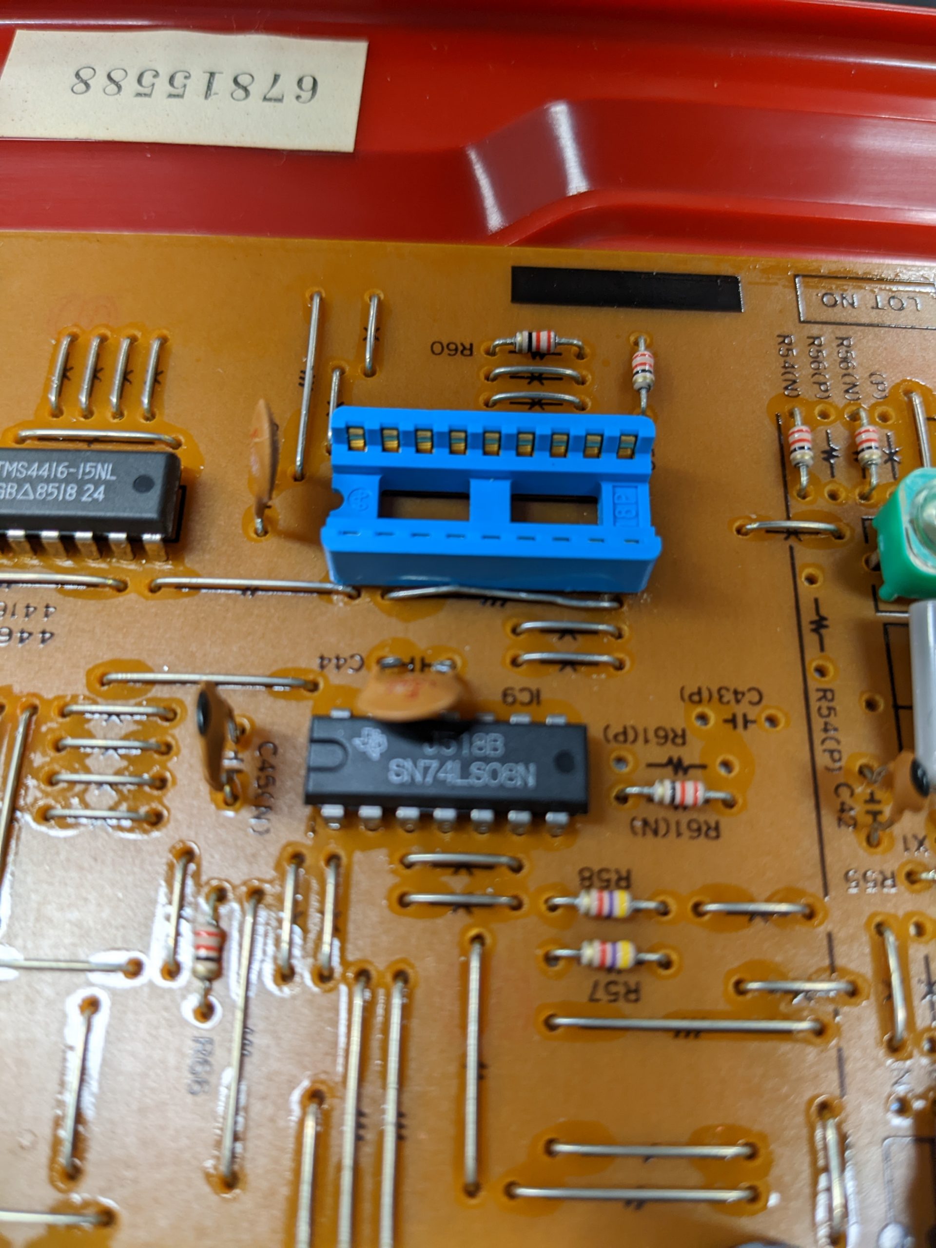
First of all, some board pics in case anyone needs them:
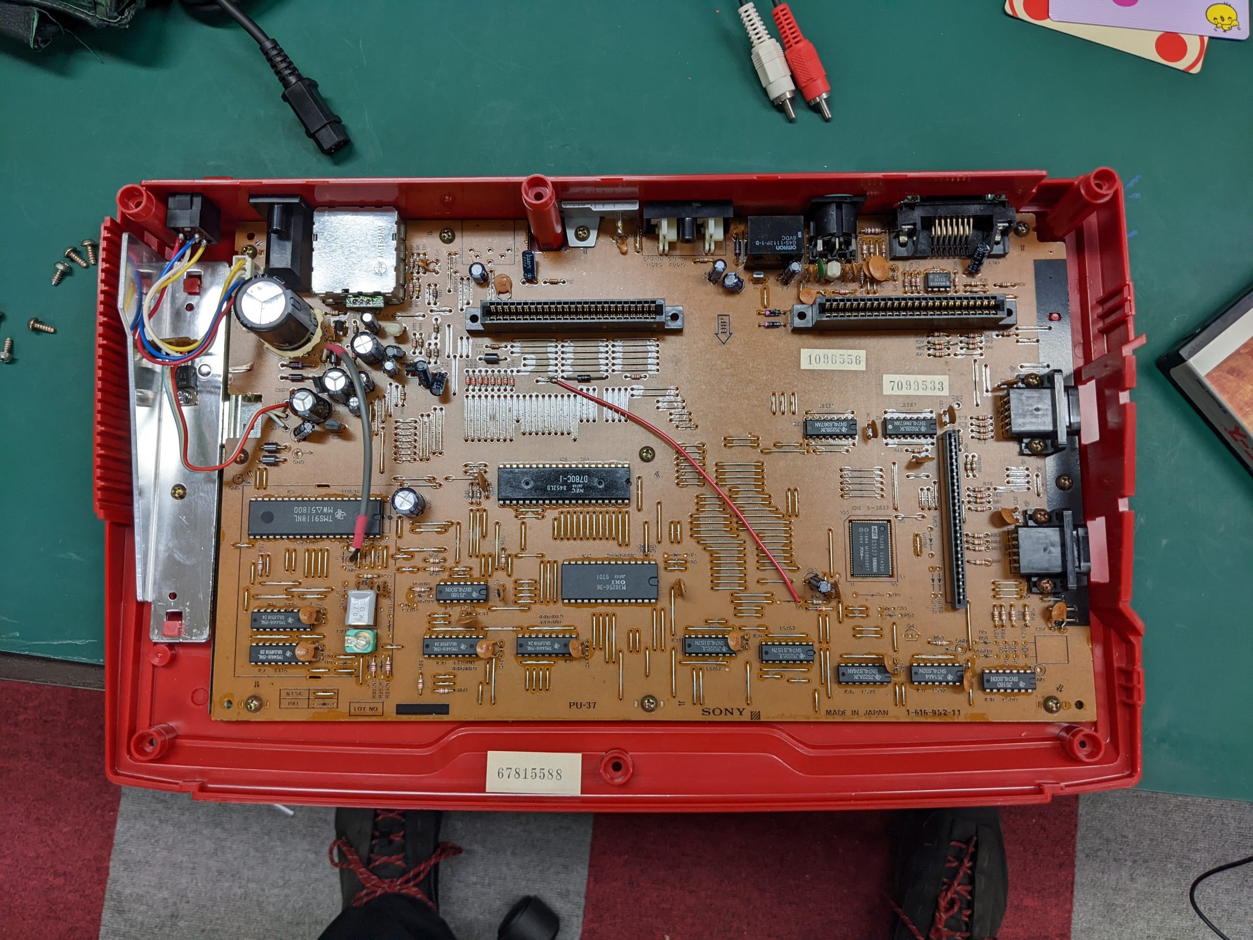

None of the chips are socketed. So let’s spy through the oscilloscope and see some worrying things:
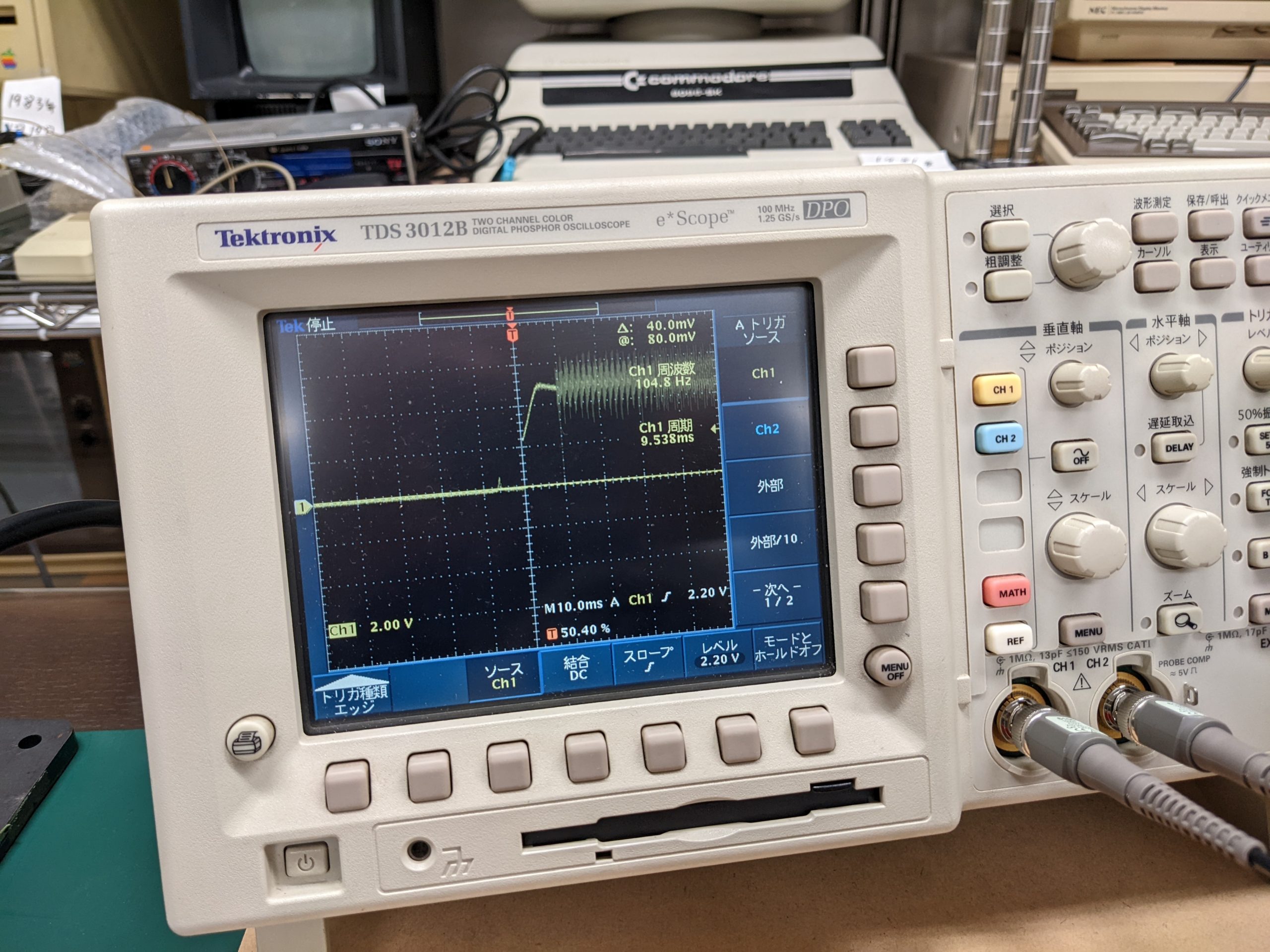
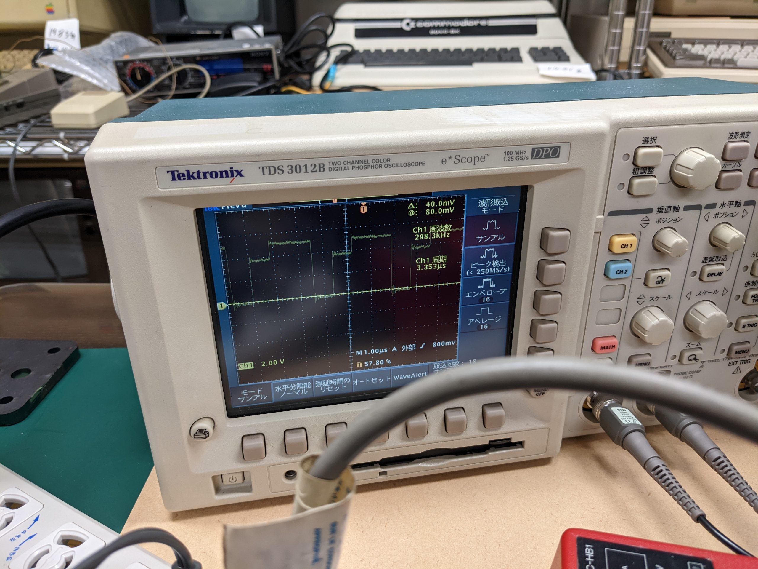
Anyway, these signals aren’t completely out of spec. (And indeed, at least the fuzzy IO turned out to be normal. I.e., this problem didn’t go away after fixing the computer. I didn’t check for the steppy address lines again after getting the computer to work, but I’d hazard a guess that they’re still there. (Update 2022/09/27: I also fixed an HB-11 a while after that, and it had the same fuzzy IO signal on the pin. Most likely nothing to worry about!)
Anyway, what we’ll do today is… build a 26-channel logic analyzer using a Raspberry Pi Pico! And a large handful of resistors to reduce the 5V signals to 3.3V. We connect the logic analyzer to the ROM chip. The ROM chip’s address and data lines are directly connected to the CPU’s address and data lines, and the RAM data lines. Except there’s no A15, but that’s probably all right for now. Using this, we may be able to figure out what’s going on. (Foreshadowing)
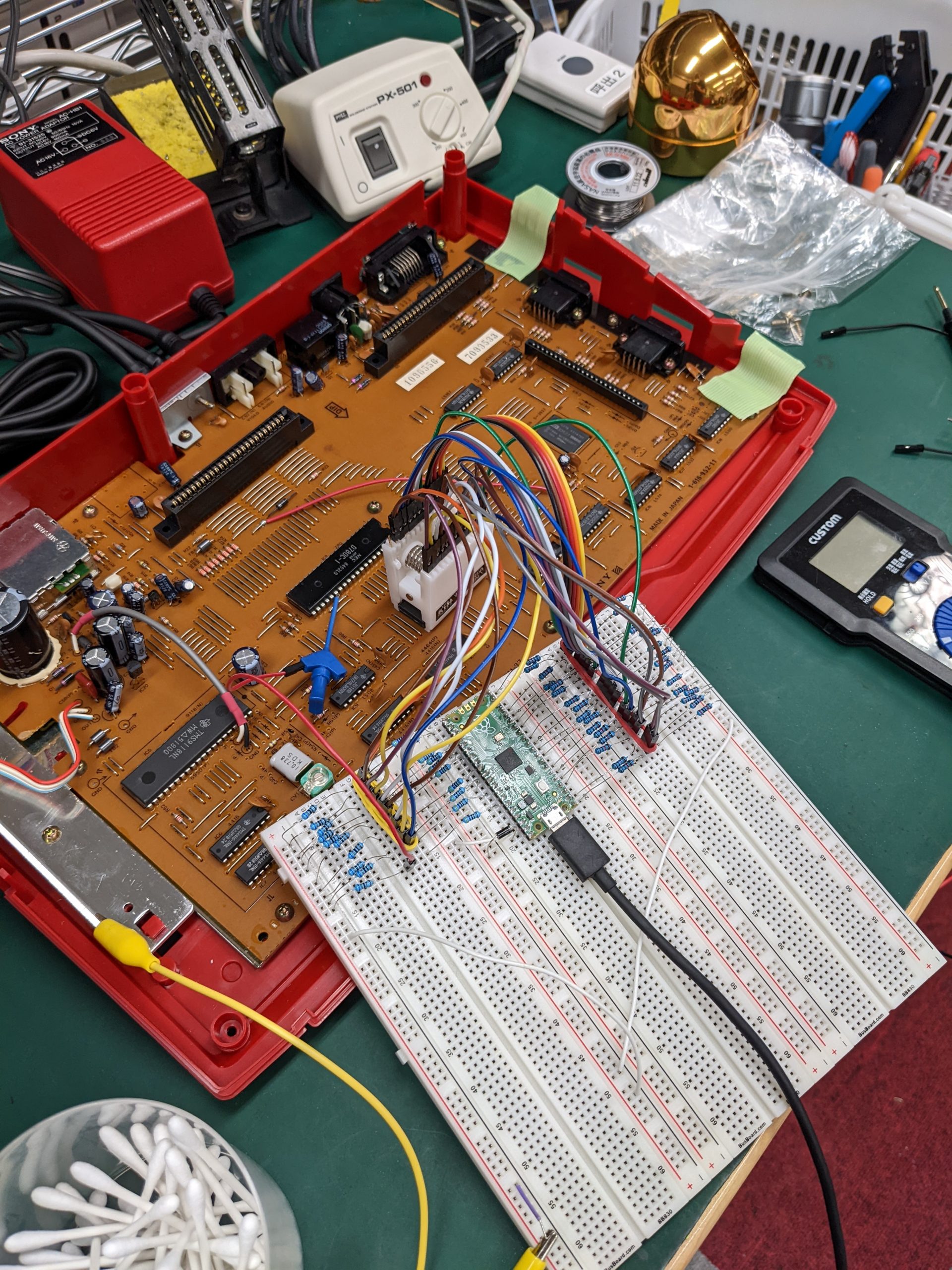
What is that awesome connector? It’s this: https://akizukidenshi.com/catalog/g/gC-04756/.
And this is the program we’ll run on the Pico:
#include <stdio.h>
#include "pico/stdlib.h"

#define ALL_REGULAR_GPIO_PINS 0b00011100011111111111111111111111
#define LOGIC_BUFFER_LEN 62660

#define TRIGGER_PIN 28

uint32_t logic_buffer[LOGIC_BUFFER_LEN] = { 0 };

int main() {
    int i = 0;
    stdio_init_all();
    gpio_init_mask(ALL_REGULAR_GPIO_PINS);
    gpio_init(PICO_DEFAULT_LED_PIN);
    gpio_set_dir_masked(ALL_REGULAR_GPIO_PINS, GPIO_IN);
    gpio_set_dir(PICO_DEFAULT_LED_PIN, GPIO_OUT);

    // wait until /dev/ttyACM0 device is ready on host
    for (i = 0; i < 10; i++) {
        gpio_put(PICO_DEFAULT_LED_PIN, i%2==0);
        sleep_ms(500);
    }
    gpio_put(PICO_DEFAULT_LED_PIN, 1);
    printf("Logic analyzer ready, waiting for trigger\n");
    while (gpio_get(TRIGGER_PIN) == 0);
    for (i = 0; i < LOGIC_BUFFER_LEN; i++) {
        logic_buffer[i] = gpio_get_all() & ALL_REGULAR_GPIO_PINS;
    }
    printf("Done recording");
    for (i = 0; i < LOGIC_BUFFER_LEN; i++) {
        printf("%04x %04x\n", i, logic_buffer[i]);
    }
    printf("Done printing\n");
}
The TRIGGER_PIN is connected to the RESET line of the Z80. The while(gpio_get(TRIGGER_PIN) == 0) waits for this line to go high. (It’s active-low.) Then we just have a for loop that fills the logic_buffer array with the contents of the GPIO pins that we are using. (I.e., all 26 “normal” GPIO pins.)
Then there’s another for loop, which prints out the contents of the buffer.
Let’s avoid spaghetti wiring, and instead prioritize connection convenience. Which unfortunately means that the GPIO pin numbers and address/data line numbers will be pretty much shuffled now. Which means that we need something to decode the output of the logic analyzer to tell us the contents of the address bus and the data bus. And this is a quick and dirty Perl program to do that. Input is on standard input. The bold lines mean that A14 is on GPIO5, A13 on GPIO4, A12 on GPIO11, etc. D7 is on GPIO22, D6 is on GPIO21, etc.
In the unlikely event that you are reading this, and in the unlikelier event that you are thinking of building this thing, I strongly recommend you connect everything in a way that is convenient for you, and fix the values in these bold lines.
#!/usr/bin/perl

# logic_analyzer_raw2address.pl

@address_positions_from_a14 = (5, 4, 11, 1, 27, 2, 3, 12, 13, 14, 15, 10, 6, 7, 8);
@data_positions_from_d7 = (22, 21, 20, 19, 18, 17, 16, 9);

while (<>) {
    $address = 0;
    $data = 0;
    $num = hex($_);
    $current_address_pin = 14;
    foreach (@address_positions_from_a14) {
        if ($num & (1 << ($_))) {
            $address |= (1 << $current_address_pin);
        }
        $current_address_pin--;
    }
    $current_data_pin = 7;
    foreach (@data_positions_from_d7) {
        if ($num & (1 << ($_))) {
            $data |= (1 << $current_data_pin);
        }
        $current_data_pin--;
    }
    printf ("%04x %02x\n", $address, $data);
}
And the other way round, address&data to logic analyzer value, which will come in handy later. Note that you need to set the input values in the source code, $address_input and $data_input. (They are set to 0x7c86 and 0x21 respectively in the below example.)
#!/usr/bin/perl

# address2logic_analyzer_raw.pl

@address_positions_from_a14 = (5, 4, 11, 1, 27, 2, 3, 12, 13, 14, 15, 10, 6, 7, 8);
@data_positions_from_d7 = (22, 21, 20, 19, 18, 17, 16, 9);

$address_input = 0x7c86;
$data_input = 0x21;

$current_position = 14;
$current_position2 = 0;
foreach (@address_positions_from_a14) {
    if ($address_input & (1<<$current_position)) {
        $mask |= (1 << $address_positions_from_a14[$current_position2]);
    }
    $current_position--;
    $current_position2++;
}
$current_position = 7;
$current_position2 = 0;
foreach (@data_positions_from_d7) {
    if ($data_input & (1<<$current_position)) {
        $mask |= (1 << $data_positions_from_d7[$current_position2]);
    }
    $current_position--;
    $current_position2++;
}
printf("%04x\n", $mask);
So, to run this, you’d do the following:
- Connect everything up, don’t forget to connect GND between the Pico and the device under test (the HB-10 in this case)
- minicom -C logic_analyzer_output -D /dev/ttyACM0
- Wait until you get the “ready” message
- Turn on the device under test
- Wait until the Pico is done printing (takes maybe two seconds)
- Turn off the device under test
- Exit minicom
- awk ‘{print $2}’ logic_analyzer_output | perl logic_analyzer_raw2address.pl > logic_analyzer_output_decoded
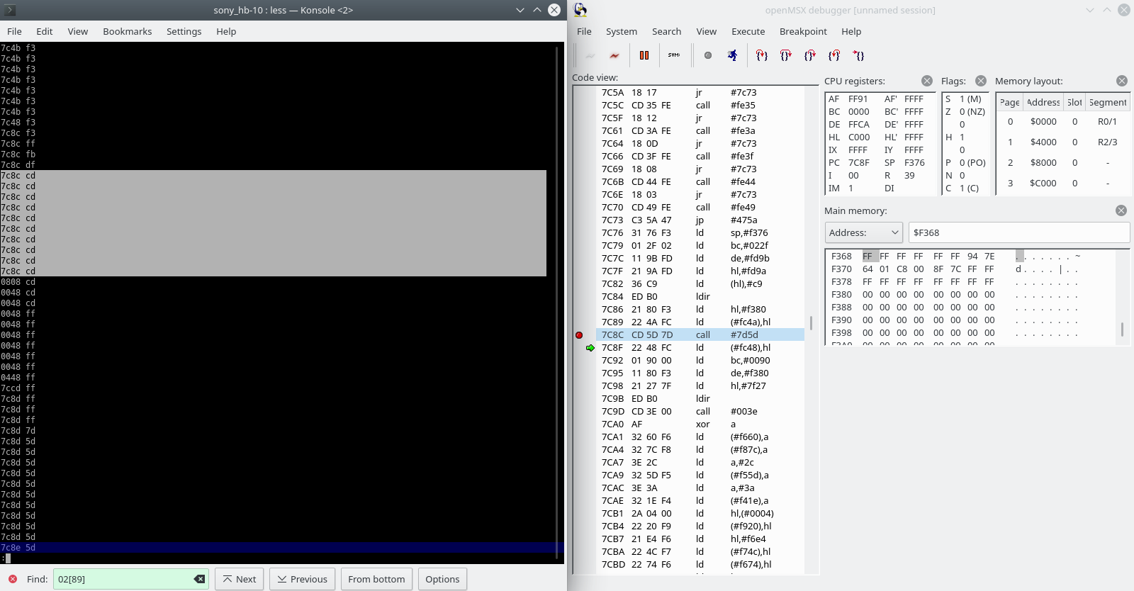
- Run openmsx and openmsx-debugger and display logic_analyzer_output_decoded side-by-side
So what do you do if you have reached the end of your trace and would like to see what happens next? In my case I saw that we spent a lot of time in a tight loop initializing memory. That takes up the entire logic buffer. So I’d like to continue reading at a certain address (which can be determined easily by following along in openmsx-debugger), right after the memory is initialized.
That’s where the other Perl script comes in. You think of an address bus value and data bus value where you’d like to continue tracing, and convert that into a value that would be seen by the logic analyzer. Then you modify the logic analyzer program like this, for example:
#include <stdio.h>
#include "pico/stdlib.h"

#define ALL_REGULAR_GPIO_PINS 0b00011100011111111111111111111111
#define LOGIC_BUFFER_LEN 62660

#define ADDRESS_PINS 0b00001000000000001111110111111110
#define DATA_PINS    0b00000000011111110000001000000000
#define ADDRESS_DATA_PINS (ADDRESS_PINS | DATA_PINS)

#define AFTER_MEMCPY 0x27d3cc
#define AFTER_MEMCPY2 0x8101af2

#define TRIGGER_PIN 28

uint32_t logic_buffer[LOGIC_BUFFER_LEN] = { 0 };

int main() {
    int i = 0;
    stdio_init_all();
    gpio_init_mask(ALL_REGULAR_GPIO_PINS);
    gpio_init(PICO_DEFAULT_LED_PIN);
    gpio_set_dir_masked(ALL_REGULAR_GPIO_PINS, GPIO_IN);
    gpio_set_dir(PICO_DEFAULT_LED_PIN, GPIO_OUT);

    // wait until /dev/ttyACM0 device is ready on host
    for (i = 0; i < 10; i++) {
        gpio_put(PICO_DEFAULT_LED_PIN, i%2==0);
        sleep_ms(500);
    }
    gpio_put(PICO_DEFAULT_LED_PIN, 1);
    printf("Logic analyzer ready, waiting for trigger\n");
    while (gpio_get(TRIGGER_PIN) == 0);
    while ((gpio_get_all() & ADDRESS_DATA_PINS) != AFTER_MEMCPY2);
    for (i = 0; i < LOGIC_BUFFER_LEN; i++) {
        logic_buffer[i] = gpio_get_all() & ALL_REGULAR_GPIO_PINS;
    }
    printf("Done recording");
    for (i = 0; i < LOGIC_BUFFER_LEN; i++) {
        printf("%04x %04x\n", i, logic_buffer[i]);
    }
    printf("Done printing\n");
}
And then it’ll start tracing as soon as it sees that the relevant GPIO pins are equal to AFTER_MEMCPY2, which is just a name I came up with.
Logic analyzer output and analysis
Here are the raw traces I produced. You’d need to use the awk command above to convert them.
And here are the three relevant post-processed files:
You can see that we have a very detailed trace of the Z80’s execution. We can easily see what address is being set by the CPU, and what’s being read at or written to that address. You may also notice that we have a couple gaps in the data, which is why we needed a retake for logic_analyzer_output2. You may also be able to tell that things apparently start at 2 here.
- We can easily see that the Z80 is executing code correctly
- We can easily see that the ROM is giving us the correct code (the code is identical to what we see in the emulator)
- We see that the code is trying to switch banks (out #a8) and identify RAM, by overwriting an address and reading back the same address
- In the emulator, it finds the RAM on first try, because it’s connected on “slot 0”, same as the ROM. (Which is possible because this machine only has 16 KB of RAM and 32 KB of ROM, which is less than the 64 KB addressable by the Z80.)
- In our logic trace, it gets back a slightly different value from what it had written, which indicates that the RAM is most likely bad!
- Let’s take a look at 000-03b6_retake.txt around line 6430+, address 0365 to 036e.
- In Z80 asm, we have here:
ld hl,#fe00
ld a,(hl)
cpl
ld (hl),a
cp (hl)
cpl
ld (hl),a
jr nz,#0379 - This means that we load from #fe00, invert, write this inversion back to #fe00, compare contents of #fe00 with our inverted value, (restore original value,) and if the comparison didn’t quite work out, we jump to #0379.
- This code is run a number of times, and it shouldn’t jump to #0379 the first time. (It doesn’t in the emulator. It ought to work the first time because ROM and RAM are both in bank 0. But if the RAM is defective, the comparison will fail!)
- We can also see our loads and stores to memory in the logic analyzer:
- Line 6510: 7e00 09 (Read 09 from fe00. A15 is missing so fe00 turns into 7e00.)
- Line 6575: 7e00 f6 (Wrote f6 to fe00. That’s the inversion of 09.)
- Line 6620: 7e00 f7 (Read f7 from fe00. Last time I checked f6 and f7 weren’t equal.)
- In our third logic trace, we reach a point where a function is called (7c8c, lines 80-165 in trace) and that function attempts to return. When a function returns, it checks the stack to figure out the correct address to return to (lines 600- in trace). And again, that address doesn’t quite match the address we had written when we executed the CALL instruction! In the trace we can clearly see that it’s reading 7d8f, when it should have been 7c8f. 7d is 01111101, 7c is 01111100. So it would appear that we have a stuck bit in D0.
- So we now jump to a rather random location, which means we start to execute nonsense code.
- At some point, the nonsense code jumps to f380 (which is uninitialized RAM). (Note that the trace doesn’t have A15, so it looks like 7380.) And while we’re now completely off the rails and firmly in nonsense territory, the see that everything here appears to have D0 set!
So before we take out the RAM chip, let’s see if we can rule out any other possible malfunctions that could lead to this behavior.
- The RAM’s address pins are not connected directly to the CPU’s address bus, instead they are most likely connected via the nearby 74LS157 chips (I didn’t check TBH). Could these be the cause of this failure?
- They would have to magically produce addresses that always have D0 set; that’s very unlikely.
- When writing the return address to the stack, we should get back the correct value because the same address should be generated when reading and writing. But we’re not reading the correct value back, so it’s very unlikely that the 74LS157 is translating our addresses incorrectly.
- Some other chip is interfering with the RAM’s output
- Unlikely, as it’s just a single bit that is erroneous
- Nothing is interfering with the ROM’s output or IO outputs
- We could probably see this on the oscilloscope
Checking RAM chips with just a multimeter?
Before taking out the chip (which is quite a chore without a desoldering iron), I put my multimeter in diode mode and checked if there’s anything unusual about the chip. And there was! Putting my positive lead on ground and the negative lead on each of the data pins, I noticed that I got a different voltage drop on the pin for the suspected defective bit, 515 mV. On all others I got 462 mV. (Disclaimer: note that this is an in-circuit test and the RAM chip isn’t the only path from ground to the data pin. I also forgot to check again after removing the chip, so take this with a heap of salt.)
So let’s see what happens when we replace that RAM chip and boot!


Did you guys know that the word “Sokoban” is Japanese? I only recently realized that when I saw the game for sale somewhere. 倉庫番!
Also, the Raspberry Pi Pico is fast. 3.3V is inconvenient, but not the end of the world.