Update 2025/05/17: It turns out that connecting Rigol scopes to the network can be very useful sometimes. Apparently you can connect your Rigol directly to PulseView by doing Connect to device → Rigol DS (rigol-ds).
Update 2025/05/21: I also have access to a Siglent SDS 1202X-E, and while (AFAIK) PulseView can’t be connected to this scope, I was able to perform a binary dump (it’s in the export options) and load it in Audacity and go from there (just as described below) just fine.
In this post, we export what we see on an oscilloscope to some odd raw format, load it in Audacity and fix it up a bit, load it into PulseView, and set up a logic analyzer decoder. This is not necessarily USB-PD-specific, you can use this to turn your oscilloscope into a logic analyzer and protocol decoder, albeit with very few channels. (Note: most oscilloscopes have decoding built in for common things like I2C. But maybe PulseView’s interface is a little nicer, so this technique might help in those cases too.)
The Rigol DS1202Z-E doesn’t have USB-PD decoding built in. Too bad. Maybe it’s available in newer scopes?
USB-PD starts when a connection is made. In my case, I’d like to check up on the negotiation between a charger (source) and a Raspberry Pi 5 (sink). It’s likely that the Raspberry Pi 5’s USB-PD negotiation is defective, but that’s a topic for another post.
USB-PD works with a really low voltage level, which most logic analyzers probably don’t support directly. Oscilloscopes aren’t that picky, fortunately. All we have to do is set up a trigger on the right voltage, with a time base that will allow us to get as much data as possible (I went with 100 ms for now).
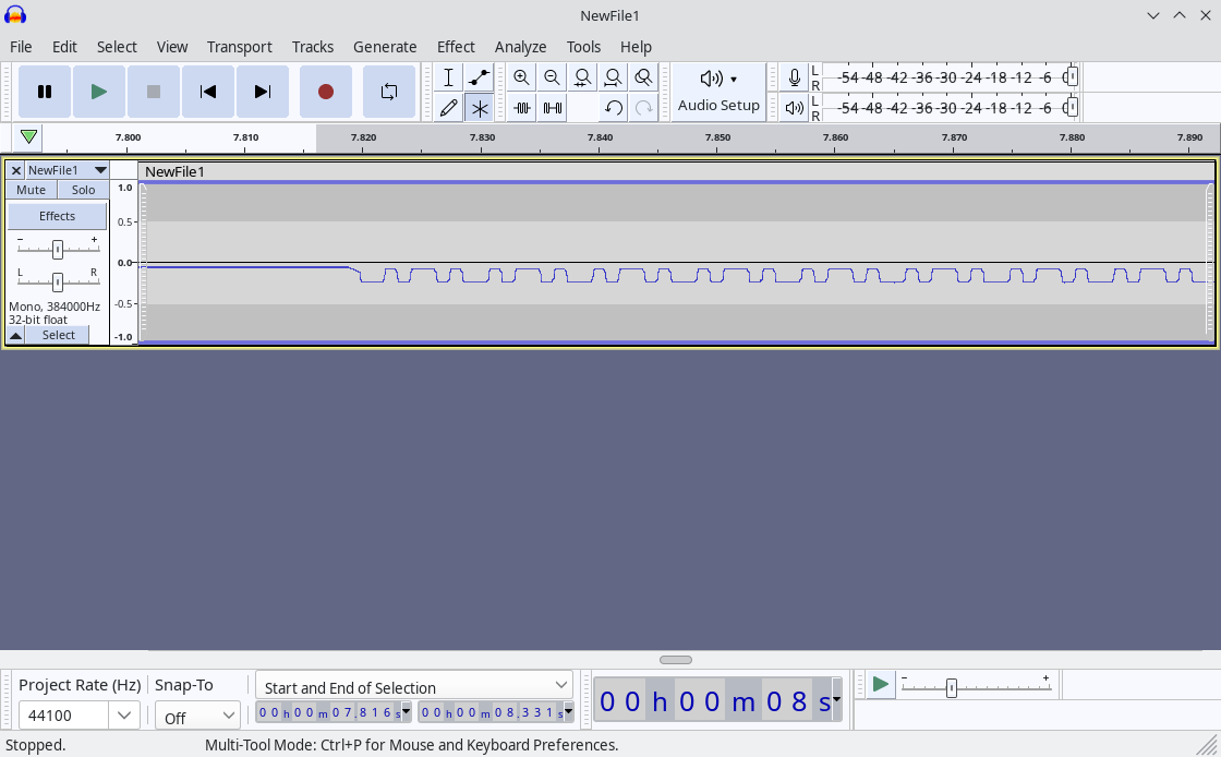
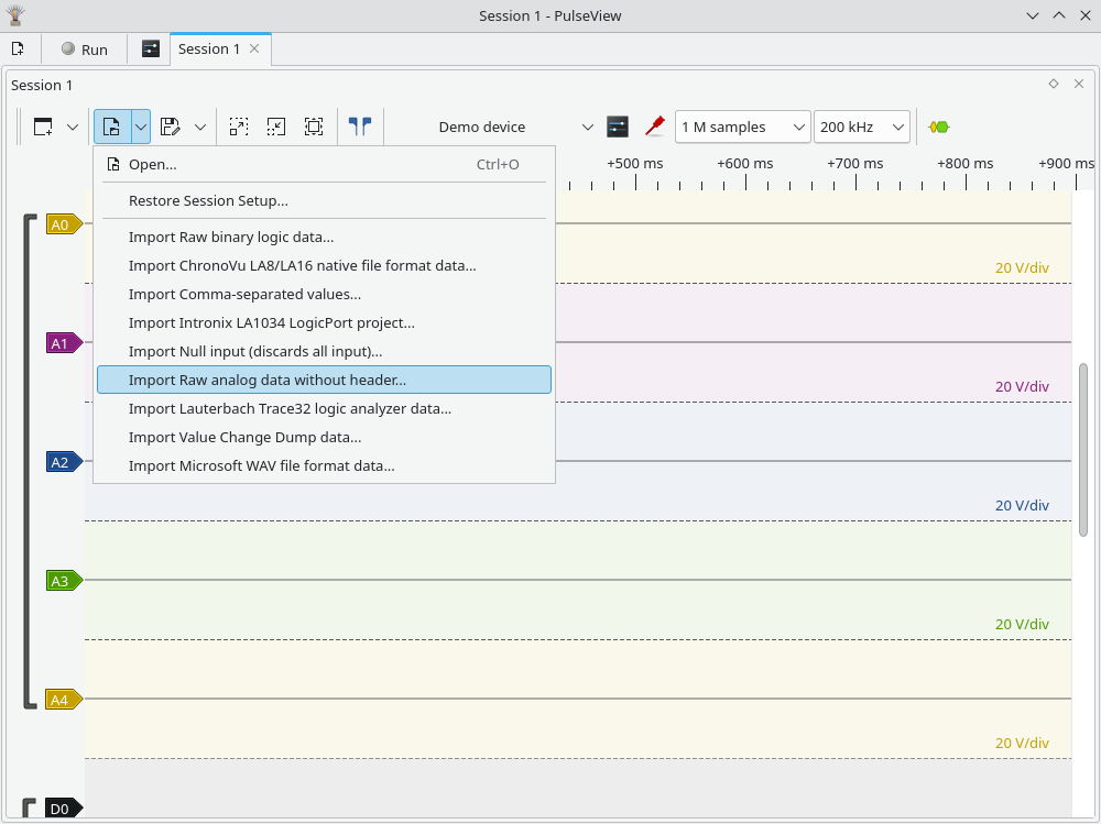
We need to store this data on a USB stick. The Rigol DS1202Z-E supports “CSV”, “TRC”, “WFM”, and probably a couple others. As you may have found out by now, getting it to save a CSV file with the entire memory takes a long time, so let’s not use that. Instead, we’ll use WFM. Done. How do we open this WFM file? We open it in Audacity! File → Import → Raw Data → NewFile1.wfm. Pick “Unsigned 8-bit PCM”, “Default endianness”, “1 channel (mono)”, start offset 0, amount to import 100%, sample rate: whatever you like. The actual sample rate is obviously incredibly high and audio sample rates are incredibly low, so I don’t think Audacity supports entering 200 MHz. (All right, I entered 200000000 Hz but it turned that into 384 KHz, I think. 200 KHz works BTW!) You should now be able to see in Audacity the wave form you saw on your oscilloscope, like this:
Imported at 44100 Hz.
What you need to do beyond this point depends on what you want to do. Duh! Well, I want to decode USB-PD. So here’s what I did next:
Next, we cut off any sections we don’t need (select using mouse and press “Del” key).
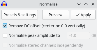
Next, we remove the DC offset (Effect → (Volume and Compression →) Normalize → Remove DC offset (center on 0.0 vertically), uncheck “Normalize peak amplitude”). (In newer versions the “Effect” menu is sorted by category, in older versions it isn’t.)
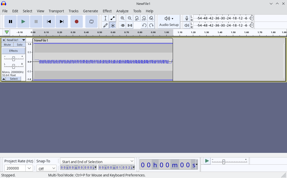
Much better!
Next, maybe amplify the signal a bit, if you like. (Effect → (Volume and Compression →) Amplify
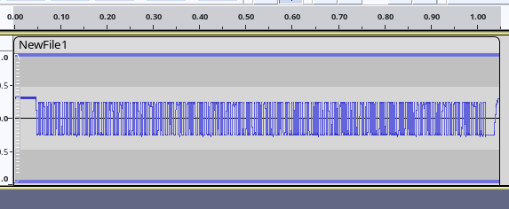
Amplified.
Next, go to File → Export → Export as WAV, select “Signed 16-bit PCM” and save as a .wav file.
Next, open this file in PulseView, but not as a WAV file, but as a raw file, like this:
Note: files ending in .wav will not show up in the file selector, so choose Filter: All Files. Data format is S16_LE, number of channels is 1, sample rate is 200000000 in my case; this depends on your oscilloscope and its settings.
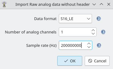
This is the result. Note that we have some junk at the beginning because of the WAV header. Feel free to get rid of it if it’s no good for your use case.
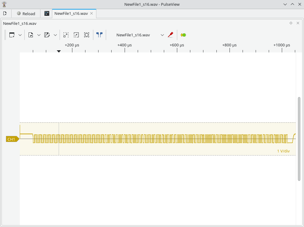
Next, click on the “CH1” arrow on the left side, set it to convert to logic, with the threshold at 0V.
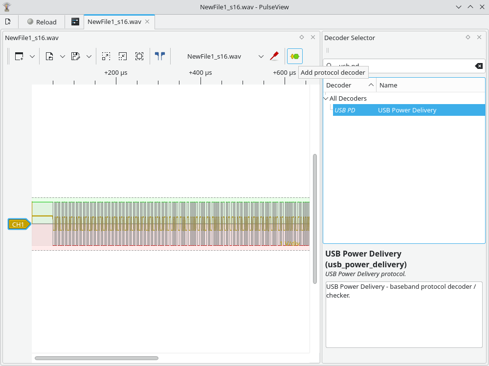
Next, we need to add the USB-PD decoder. Press the yellow/green button in the toolbar, search for “usb pd”, and double-click the “USB PD” item.
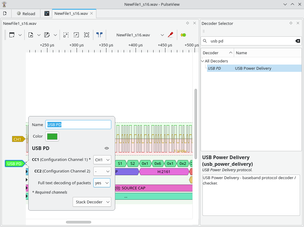
Next, press the “USB PD” arrow on the left side and set CC1 to be CH1, and optionally select “Full text decoding of packets”: yes.
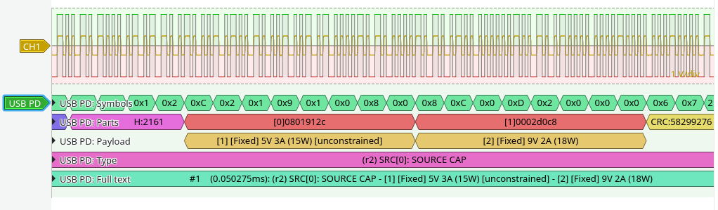
Done!This charger advertises 5V at 3A max, and 9V at 2A max. Matches exactly what it says on the charger!
Back in the days of the Apple II, you could apparently run off to Akihabara and get the same computer with possibly better components for less money. Or just the parts you needed.
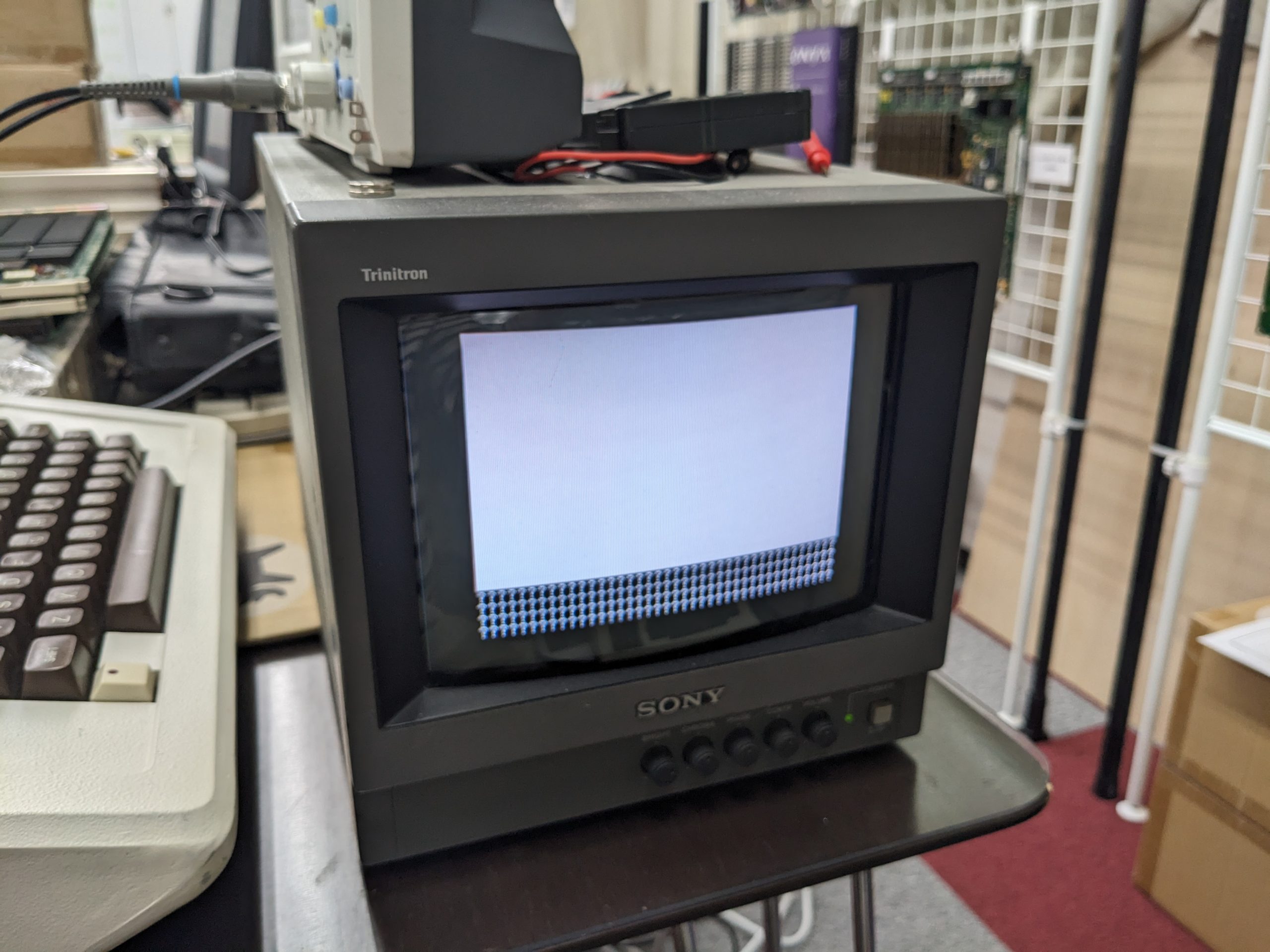
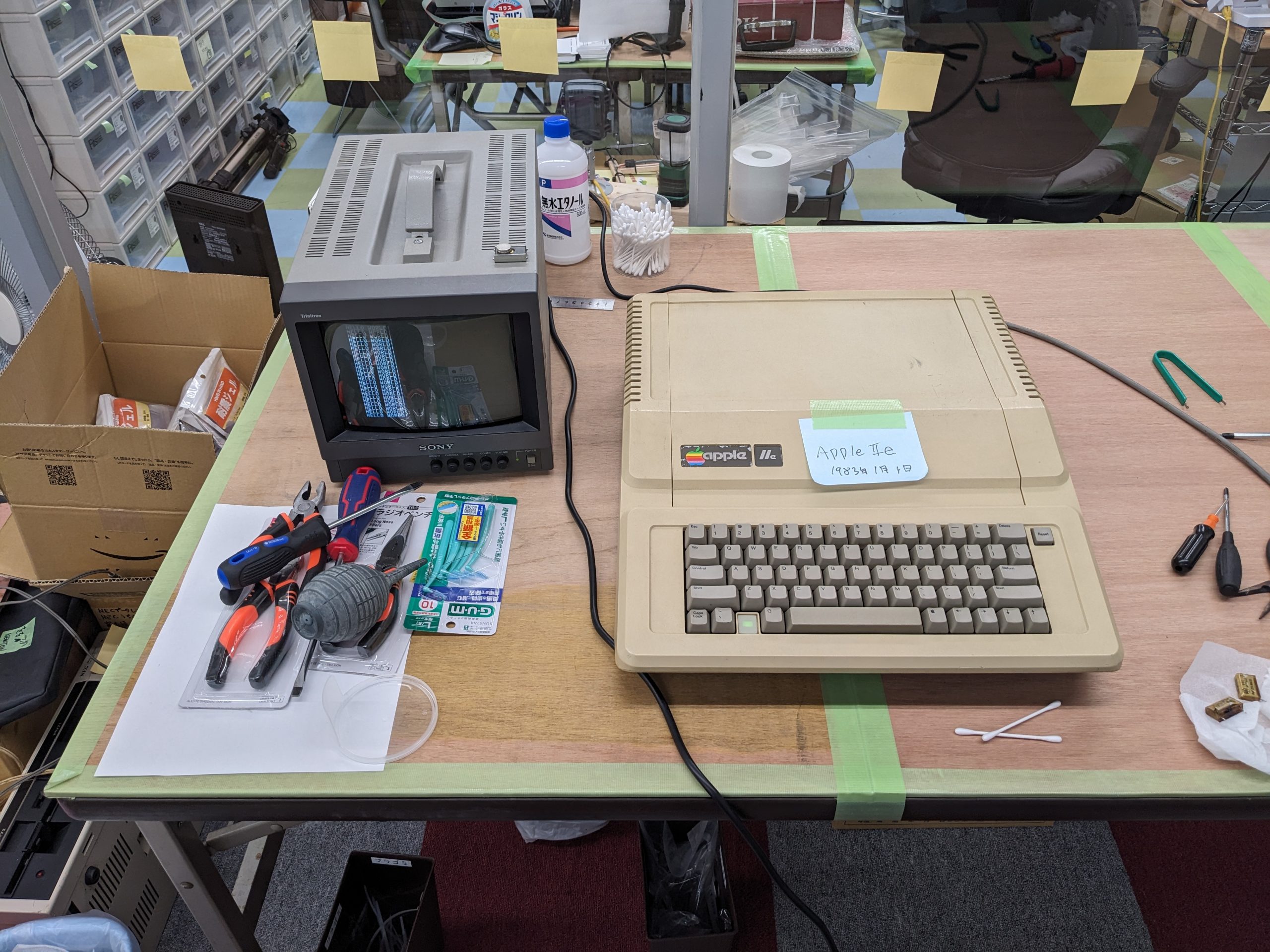
I had a chance to look at such an Apple II Plus clone that wouldn’t boot into BASIC. It beeped and displayed “Apple ][” at the top, but didn’t go anywhere from there. Pressing Ctrl+Reset made it produce another beep, but nothing happened on the screen. Sometimes it beeped twice. Once in a blue moon it would enter the monitor. And as I found out through trial and error, it would also enter the monitor when I pressed Ctrl while turning on the power switch on the PSU.
Before I did that though, I checked the voltages, and they were pretty low, near 4.6V, even with all expansion cards removed! (I also checked for hot spots to make sure there were no almost-shorts.) Fortunately the PSU supplied in this computer has a potentiometer that allows users to adjust the voltage without even opening the computer!
When you’re in the monitor you can check the memory, ROM, and do what you want! And since this is a popular system, you’re just one Google search away from getting some really cool incantations that you can paste^Wpeck in there.
For example, I found something that’ll perform a memory test! This test passed with flying monochrome colors.
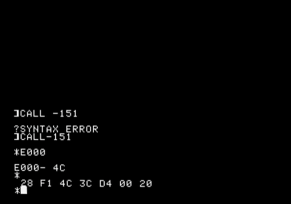
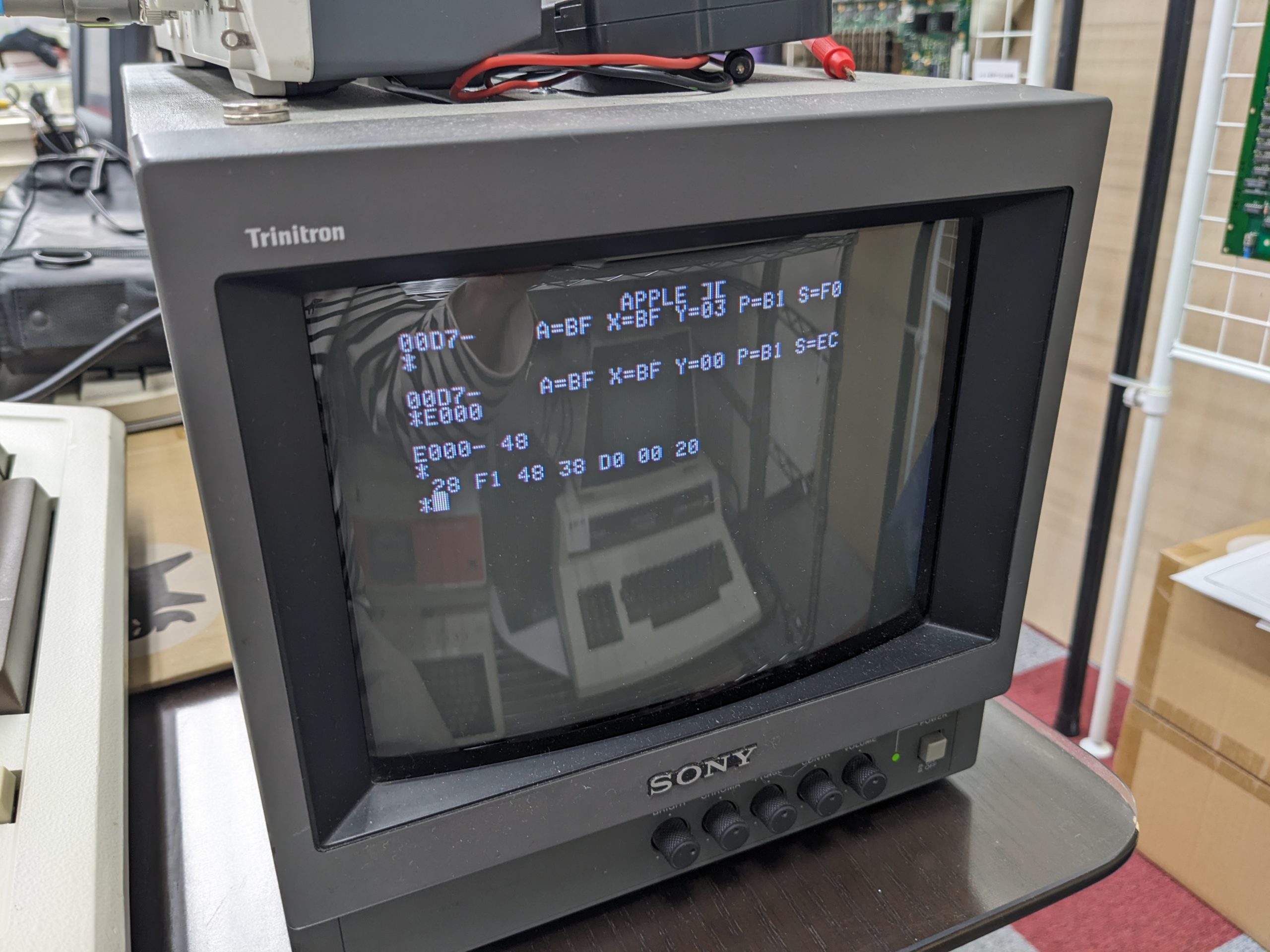
If the RAM is good, the ROM could be bad, or there might be a problem with a buffer chip, etc. So how do you test the ROM? Well, you go to https://www.scullinsteel.com/apple2/ on a computer (or phone), select the appropriate machine (][+ in this case) and enter the monitor by typing “CALL -151” (or “CALL-151”?). Then you type, e.g., “D000[return][return]”, and you’ll get the contents of the ROM at D000-D007. I had a look at the first 8 bytes of D000, D800, E000, E800, F000, F800. And guess what? E000-E007 were different!
Emulator On the real machine
E000 has 4C in the emulator, 48 on the real machine. E003 is the same. E004: 3C/38.
0x4C is 0b1001100. 0x48 is 0b1001000. 0x3C is 0b0111100. 0x38 is 0b0111000.
As we can see, it looks like one bit is refusing to come up.
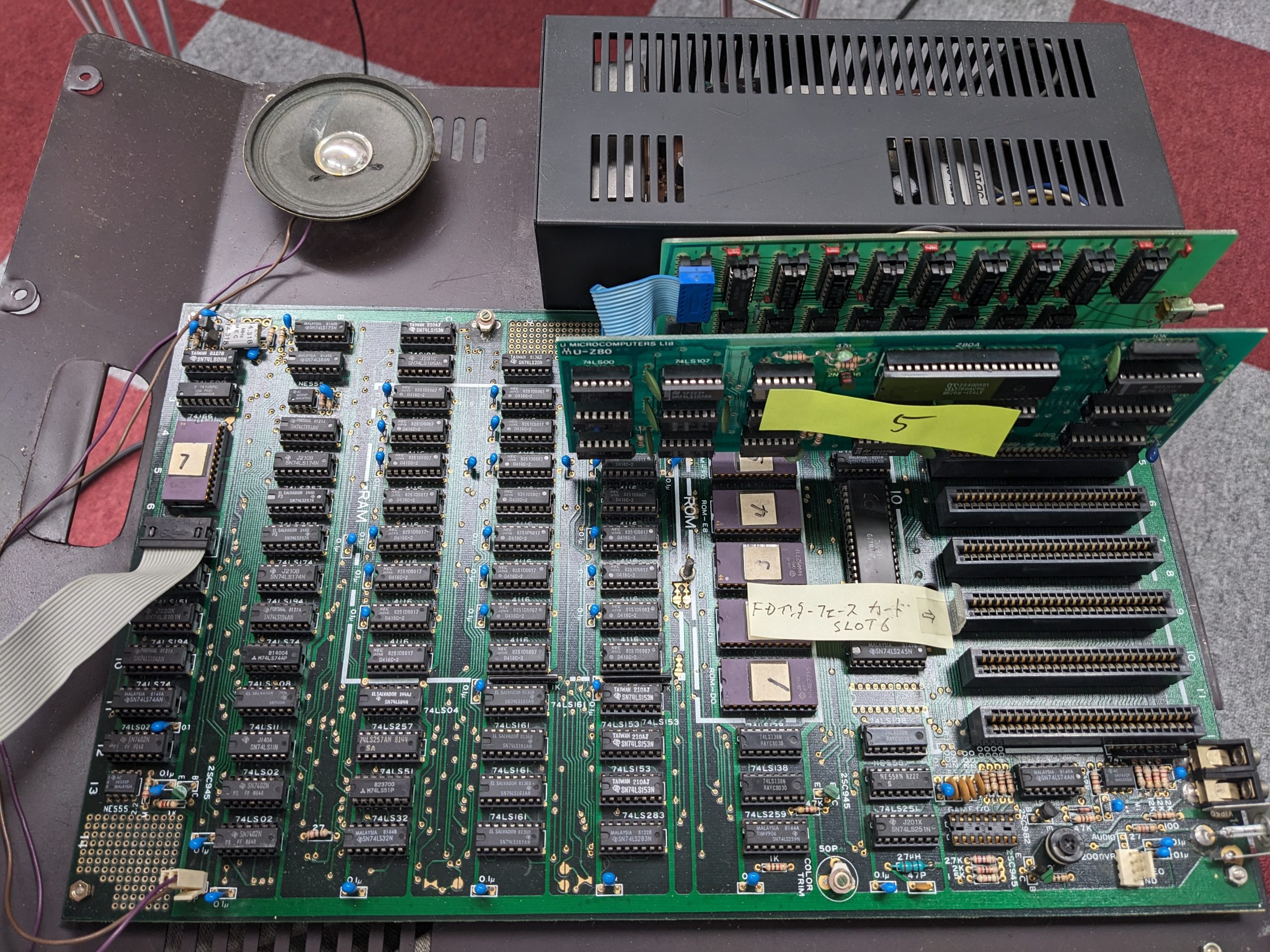
I took out the ROM for E000-E7FF (which is conveniently labeled E0 on the PCB), cleaned the pins and the socket, and put it back in. And that’s all that was wrong with it! (I’ll replace at least one cap in the power supply at a later date. Unfortunately it’s one of those huge high-voltage high-micro-Farad ones that aren’t available in my parts cabinet.)
Mainboard. The ROM chips are regular 2716 chips, which is pretty useful compared to e.g. 2316 or 2516. Plus they have gold-plated pins! There was no crustiness at all.
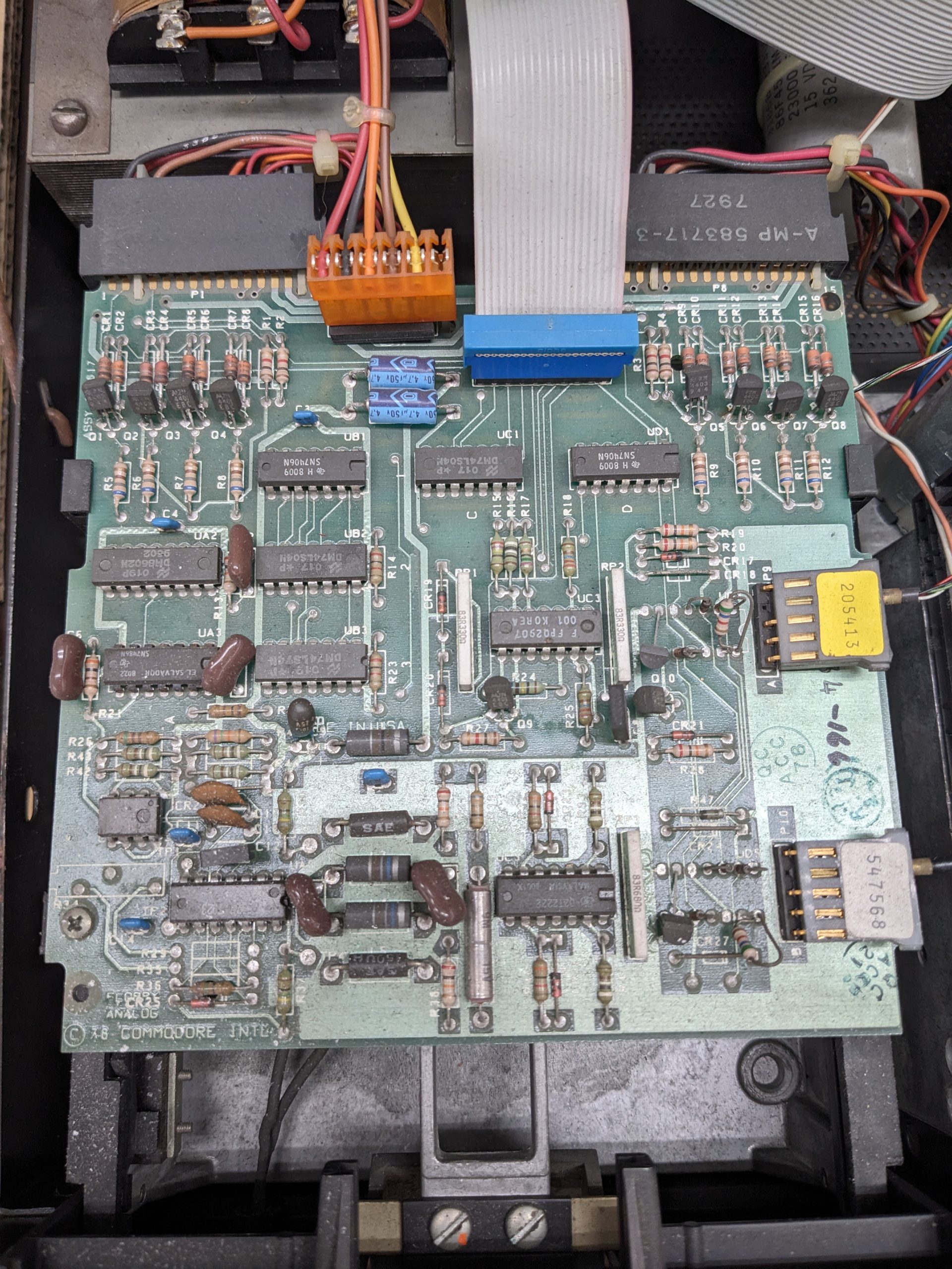
I recently had a chance to look at a malfunctioning Commodore 3040 floppy drive.
Smoke coming out of drive
There is a real chance that yours too might emit magic smoke when you turn it on for the first time in decades. So before turning it on, be prepared to turn it off quickly, and then watch it like a hawk. Reacting quickly may prevent shorted tantalum capacitors from bursting. Check the schematics and BOM to see what kind of capacitor to use. (You’ll find all that at https://www.zimmers.net/anonftp/pub/cbm/schematics/drives/old/index.html)
The tantalum capacitor a little left to the center of the board (right over the “MADE” part of “MADE IN USA”) is all black, but hasn’t exploded.
Cleaning
Clean the heads. And if the drive looks really dirty on the inside (the case isn’t exactly dust-proof), do some general cleaning perhaps. It also makes it nicer to work on it!
Maybe move the head position manually a couple times, just to make sure the mechanism is not stuck.
It would probably be best to unplug all connectors and clean them. I did that for most. Before that, the drive would often just stop responding to commands.
PEBKAC #1
Being more accustomed to the Commodore 64’s 1541, I assumed you could just do LOAD “$”,8. Well, you can’t with early versions of BASIC and/or the DOS. You first have to make the drive read in the BAM. This is on the 18th track, first sector. And the drive currently doesn’t even know what track it’s on, so you must initialize it. So assuming that you want to talk to “drive 0”, (the 3040 has two drives, 0 and 1) the first command you execute (in BASIC’s normal interactive mode) is:
OPEN 1,8,15,”I0″ And then: CLOSE 1
(For drive 1 it’s OPEN 1,8,15,”I1″)
If you get an error light, which I did, you probably won’t succeed in getting a directory listing either. There’s an incantation you can use to get the drive’s error message, but it’ll likely just be “READ ERROR”:
10 OPEN 1,8,15 20 INPUT#1,A,B$,C,D 30 PRINT A;B$;C;D 40 CLOSE 1
Fixing the drive speed
The PET drives are belt-driven. The speed is controlled by a potentiometer on a small board attached to the drive. The belt is on the back side, and there is an indicator that helps determine if the drive is running at the right speed. This indicator works if you have lighting that goes on and off at 50 Hz (or 100 Hz or some other multiple) or 60 Hz (or 120, etc.). In the age of LED lighting, that will likely not be the case. If you want to know what frequency your light oscillates at, just use an infrared LED (a red or green LED will likely be fine too, or even other colors) and attach its pins to your oscilloscope probe’s GND and signal (it’s a floating device, so it doesn’t matter which way you connect it). If you hold the LED close to the light source, you should see an oscillating voltage and your oscilloscope will show it’s frequency.
Or… just attach an LED to a microcontroller and turn it on and off at the correct frequency.
Anyway, my drive speed was out of whack but in my case the potentiometer was just dirty perhaps. Moving it left and right a little bit fixed the issue.
Running drive diagnostics
Having logic diagnostics on a floppy isn’t very useful if the floppy drive doesn’t work, so let’s convert it to a wav file that we can play through the datassette drive with a 3.5mm to tape converter inside. Grab cbm_technician_disk.d80 from the aforementioned site, and use VICE’s c1541 program to run this:
Maybe VICE can do it too, but I use a program called prg2wav (https://wav-prg.sourceforge.io/) to convert this to a WAV file. I have some more explanations on how to use this program in this post. Just for my own notes, here’s the command I use to run the program:
If the test goes well, the floppy drive’s LEDs will blink in a random pattern.
Don’t have a datassette either? Well, the program is written in BASIC so you could copy it by hand. ;)
Since they were socketed, I decided to give the 2114 SRAM chips inside the floppy drive another separate test. I made a 2114 RAM tester a couple years ago, but reused the breadboard for something else. So I just took out the 2114 chips one by one and put them in the PET’s VRAM socket. I didn’t see any issues.
PEBKAC #2
I didn’t really know whether my media was good or not, so I put it in a working 1541 drive attached to a C64, formatted it, saved a small program, and took the floppy back to the 3040. This time, the initialize command worked! So I did LOAD “$”,8. The drive said it was loading, but never finished. (Also the LEDs were doing something weird?) After that, I tried formatting the disk again (on the 3040), and it finished without errors! However, LOAD “$”,8 still didn’t work.
At this point I decided to read up on how Commodore floppy drives actually worked. I found a book called “Inside Commodore DOS” and put it on my Kindle and read the first few chapters on the train on my way to work and other places: https://archive.org/details/Inside_Commodore_Dos_1984_Datamost_a
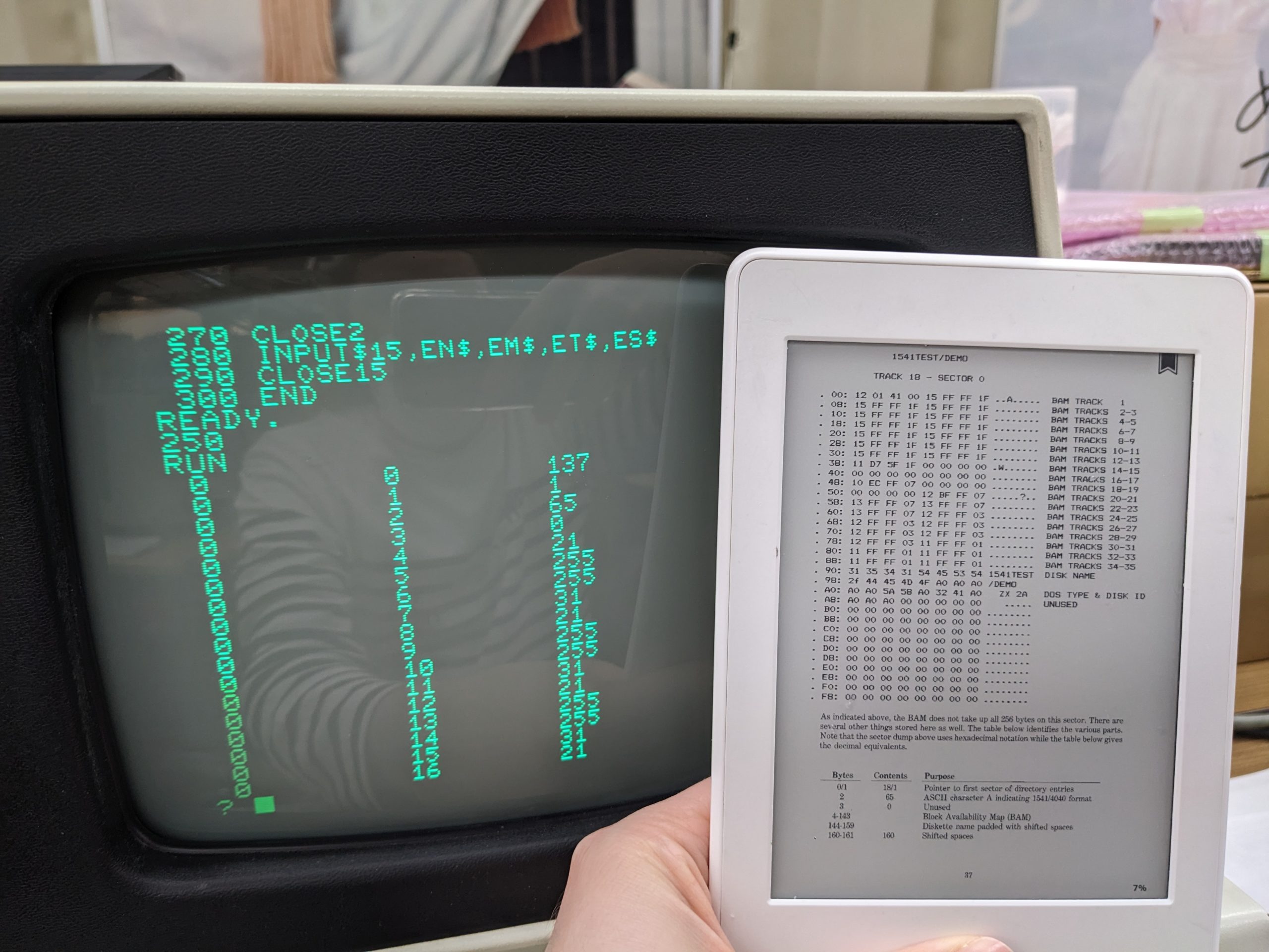
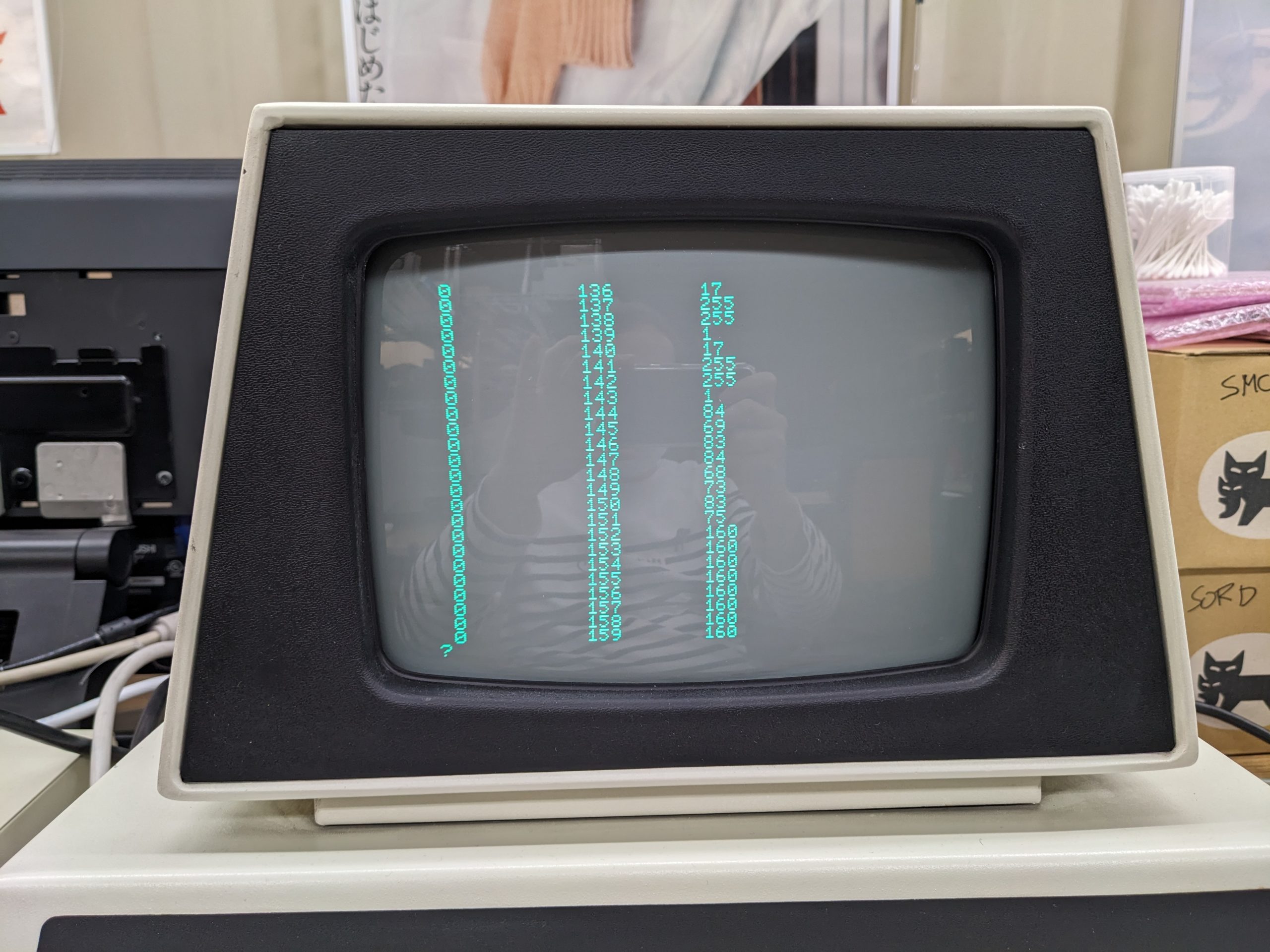
This book is mostly about the 1541, but most things didn’t change much, and it does mention some things specific to older drives as well. It explains how the BAM/filesystem works, and includes short example programs that do ~mid-level sector reads and print the result on the screen. I ran the program in chapter 5.3 (“Block-Read Command (U1)”) on page 74. And to my surprise, I got a decent result! The magic numbers looked plausible and the disk name (specified when formatting) too!
Verifying the first 16, er, 17 bytes. Note that the very first byte is different. But perhaps that’s just due to a DOS version difference? (Also you need to convert decimal to hex in your head.)Bytes 144-159 are the disk label specified when formatting. perl -e ‘printf “%c”, $_ for 84, 69, 83, 84, 68, 73, 83, 75’ => TESTDISK. Yay!
Next, I tried something that was mentioned earlier in the book… On the C64 you usually do LOAD “$”, 8, sure. But you can also do LOAD “$0”,8. The book said that this is a relic from earlier times when there were two drives per drive. And the 3040 obviously is from those earlier times! So the correct commands are…
LOAD “$0”,8 SAVE “0:FILENAME”,8 VERIFY “0:FILENAME”,8 LOAD “0:FILENAME”,8
And guess what, these commands fricking worked! Dammit.
Except the drive sometimes get stuck somehow, but that’s a topic for another day. (It seems like it’s in the communication part. I can turn the drive off and BASIC will return with a DRIVE NOT PRESENT error.)
All emulators included in the Common Source Code Project that I’ve tested work in Wine (so far: tk85.exe, pc8001.exe, smc777.exe)
ROMs are not included, but you can get many ROMs from various ROM sites
PC-8001
Search for e.g., ‘pc-8001 mame rom’. At the time of this writing the first result is a page from wowroms.com with the required files
In the binary/ directory, there is a file called pc8801.txt with a list of file names of ROM files that the software will look for. The wowroms.com zip file contains the following files (random-looking number in front of the file name is the MD5 sum): cbf25d28f7f23ea3313c82587f873cd1 ap2k.ic3c cd428f9ee8ff9f84c60beb7a8a0ef628 font.rom 2e47e5a78ad3c84ee4e782a1e2d887f9 it.em.ou.bin 37f6793f7f3e3af0b506a33283a89d92 lx800.ic3c 56e4e812c7a3240af96a474240610378 lx810l.ic3c f374db2869f7f44356ede51e94b4c5b6 n80v101.rom f1f6109541a89b626d4faf3f92ce5d75 n80v102.rom 36a73378118eb9a610d50a8b5098c404 n80v110.rom 324fb3d389cc0af5cc7df4a6f5c935d0 p72.2c 26f9ac2a43dc28df74fea101c5ee1979 pl80.pt6 ead508099bf31291543f22291703bba5 tiny.bin f9e396bd8385cc70a95b70510b80f7d0 w8_pe9.9b
We want “N80.ROM for N-BASIC mode“, this is n80v101.rom in the zip file
cp n80v101.rom binary/binay_win10/N80.ROM
You can now boot (by doing wine pc8001.exe), but the characters are all white blocks.
font.rom contains bitmaps for our characters, but just renaming font.rom to KANJI1.ROM doesn’t help. Instead, do cat font.rom font.rom font.rom > binary/binay_win10/KANJI1.ROM
You should now be able to boot
PC-8801
Again, look for the ROM (search for ‘pc-8801 rom’). For the fonts, follow the steps above. (The font.rom is the same as above. If you already did the “cat font.rom font.rom font.rom > KANJI1.ROM command” you don’t have to do it again. If you haven’t, see above notes for the PC-8001.
However, you need one more file, SUBCPU.60. I couldn’t find the original ROM, and was satisfied using the compatible implementation available at this link: http://000.la.coocan.jp/p6/basic.html But I’m sure the original is floating around somewhere. (It seemed to me like it wouldn’t matter too much what code the 8049 microcontroller is running.)
SMC-777
binary/smc777.txt indicates that the following files are needed:
    SMCROM.DAT      Shadow ROM
    KANJIROM.DAT    Kanji ROM
However, only SMCROM.DAT is necessary. You should be able to find it by searching for ‘smc-777 rom’. The MD5 sum of the file is f6a34be914cd1b22e196c15e69cdd3ac. In my case it was called “smcrom.dat”, but you have to name it SMCROM.DAT and put it into the binay_win10/ directory. (Unless your OS can’t tell lower case from upper case, that is.) If you get a blinking cursor, you’re good. You can now insert floppy disks and the system will automatically boot from them.
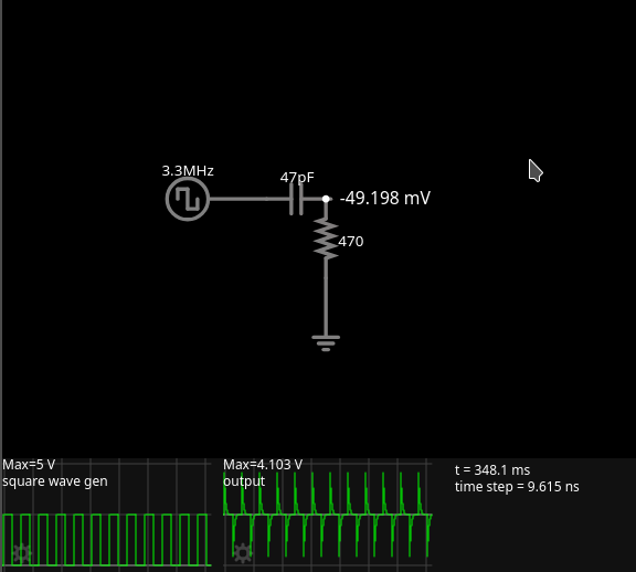
C11 is unusual in a digital circuit. Capacitors don’t pass DC. But digital circuits are DC, in a way. C11, together with R25, takes the clock signal (3.25 MHz) and mangles it.
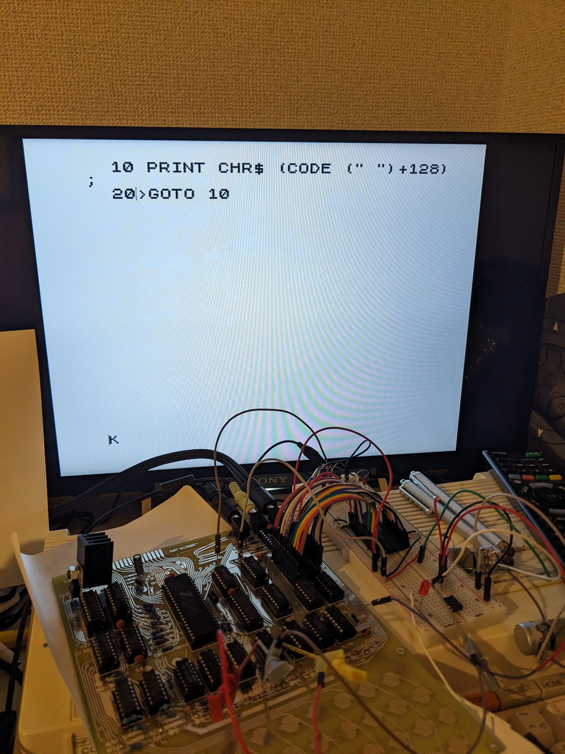
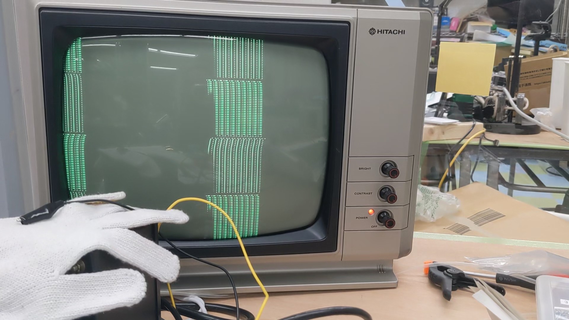
In this simulation, we turn a nice 0V-5V square wave into a spiky thing with -4.103V lows and 4.103V highs. And we send this curious signal into two 74LS logic chips, IC11 (74LS00) and IC16 (74LS10). When we look at this signal on an oscilloscope, we see a very low signal (not anywhere near 4.103V), more like -1.4V to 1.4V. Reality is probably somewhere in between. I had Texas Instruments SN74LS00N (from 2019 I think) and SN74LS10N (older markings, not sure what year) chips, and the 74LS10 one was able to see the peaks and interpret them as a logic HIGH. The 74LS00, on the other hand, never interpreted the peaks as a logic HIGH. This produced a picture where inverted characters only had the first column inverted.
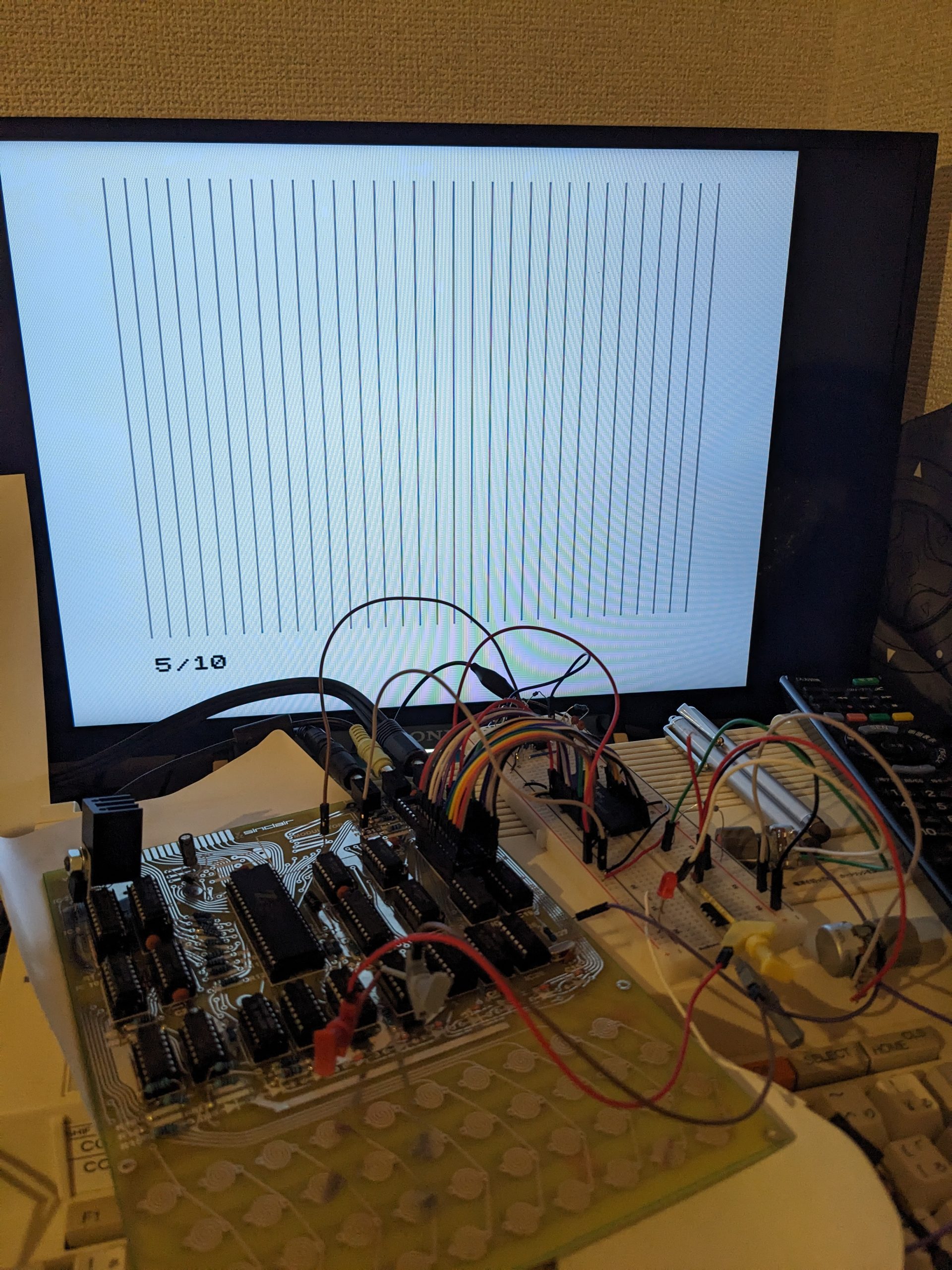
As you can see the “K” cursor has a thin vertical line in front of it. BTW, this code generates a screenful of inverted spaces.Lots of inverted spaces. Except they each consist of only a single vertical column.
I fixed this problem by buying another 74LS00. I bought one from Hitachi (now Renesas), called HD74LS00P.
Looking around the internet, some people change the capacitor, some change the resistor, some change both, some use different resistors/capacitors pairs on IC11 and IC16. I tried various things but unfortunately this didn’t work for my 74LS00. I believe the simplest solution would be to just get different 74LS00s and 74LS10s from several vendors and trying them out. And if that takes you nowhere, you could maybe try and use a couple transistors to rectify and amplify the signal. (It’s a rather fast signal so that may make it harder than just using a simple common-emitter configuration where the transistor is driven into saturation millions of times per second.)
So what is this RC filter good for anyway?
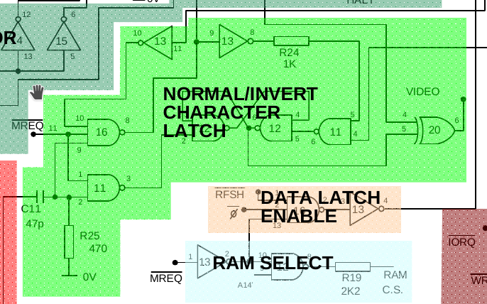
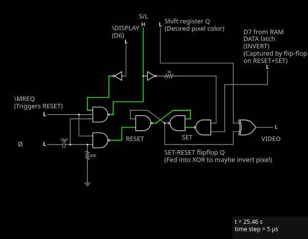
Let’s have a look at this simulation, which includes the entire “NORMAL/INVERT CHARACTER LATCH” logic:
We have an S-R flipflop implemented using two NAND gates. This flip-flop’s job is to remember the state of D7 (which only briefly remains on the data bus) for 8 pixel clock (6.5 MHz) cycles (the abovementioned 3.25 MHz clock is half the pixel clock). If we didn’t do this, only the first column of each inverted character would be inverted.
How does it do this? For the most part, it’s explained on Grant Searle’s site. Have a look at this extract, though it’s mostly concerned with IC16’s job.
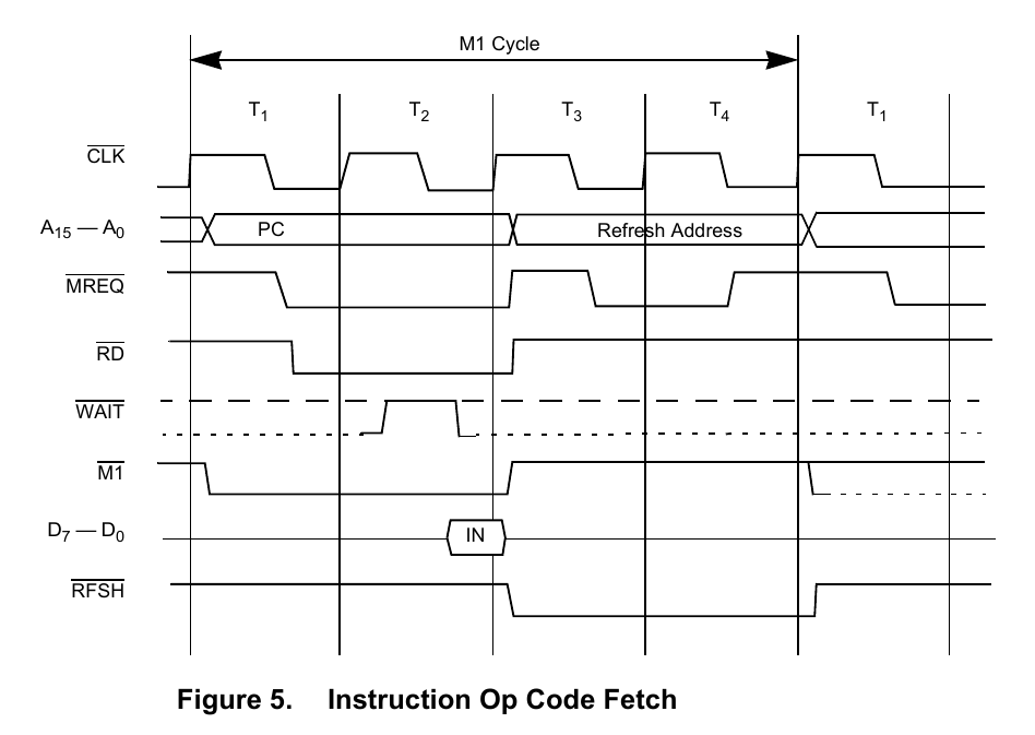
At the very end of the opcode execution (actually, the very start of the next opcode), the load pin on the register is very briefly (via a capacitor) pulsed low, to load whatever is being output on the data bus (from the ROM) into the shift register. The pulse is activated by a positive clock transition. This is only active when /MREQ is high. As you can see from the oscilloscope traces, the only time a positive transition occurs when /MREQ is high is at the start of the T1 state.A further blocking signal (into pin 10 of IC 16) ensures that the trigger pulses only occur when a character has been loaded (ie. when the NOP circuitry has been activated). This ensures that no data is loaded into the shift register at other times during the display.
The data that has been loaded is is then streamed one bit at a time (highest bit first) to the output (via the XOR IC 20, to invert if needed) and then passed directly to the TV modulator to convert the 0 and 1 levels into dark/light bits on the screen.
http://searle.x10host.com/zx80/zx80ScopePics.html
I think it might help to break things down a little further. First of all:
We want the S-R latch to be reset and set to the correct inversion state at the start of every character. On the ZX80 computer, one character is output by executing a NOP (while in \DISPLAY mode). On the Z80 CPU, a NOP is executed in 4 CPU cycles. The pixel clock is twice that speed, so we output 8 pixels in that time. Let’s look at the Z80 CPU’s NOP instruction timings:
We see our \MREQ in the third row. We see it’s already high when entering T1. It also goes high again in T3 and later in T4. But if our flip-flop is reset every time we get a high MREQ and a high clock, that would mean our flip-flop gets reset three times per character! Well, that’s where the RC circuit comes into play:
On one side of the capacitor, we have the CLK signal. On the other side of the capacitor, we see a really spiky signal that just goes up for a split microsecond and goes down again, and stays down (or goes down further than required, but that’s… okay). In other words, C11 and R25 implement this bit: “The pulse is activated by a positive clock transition.“
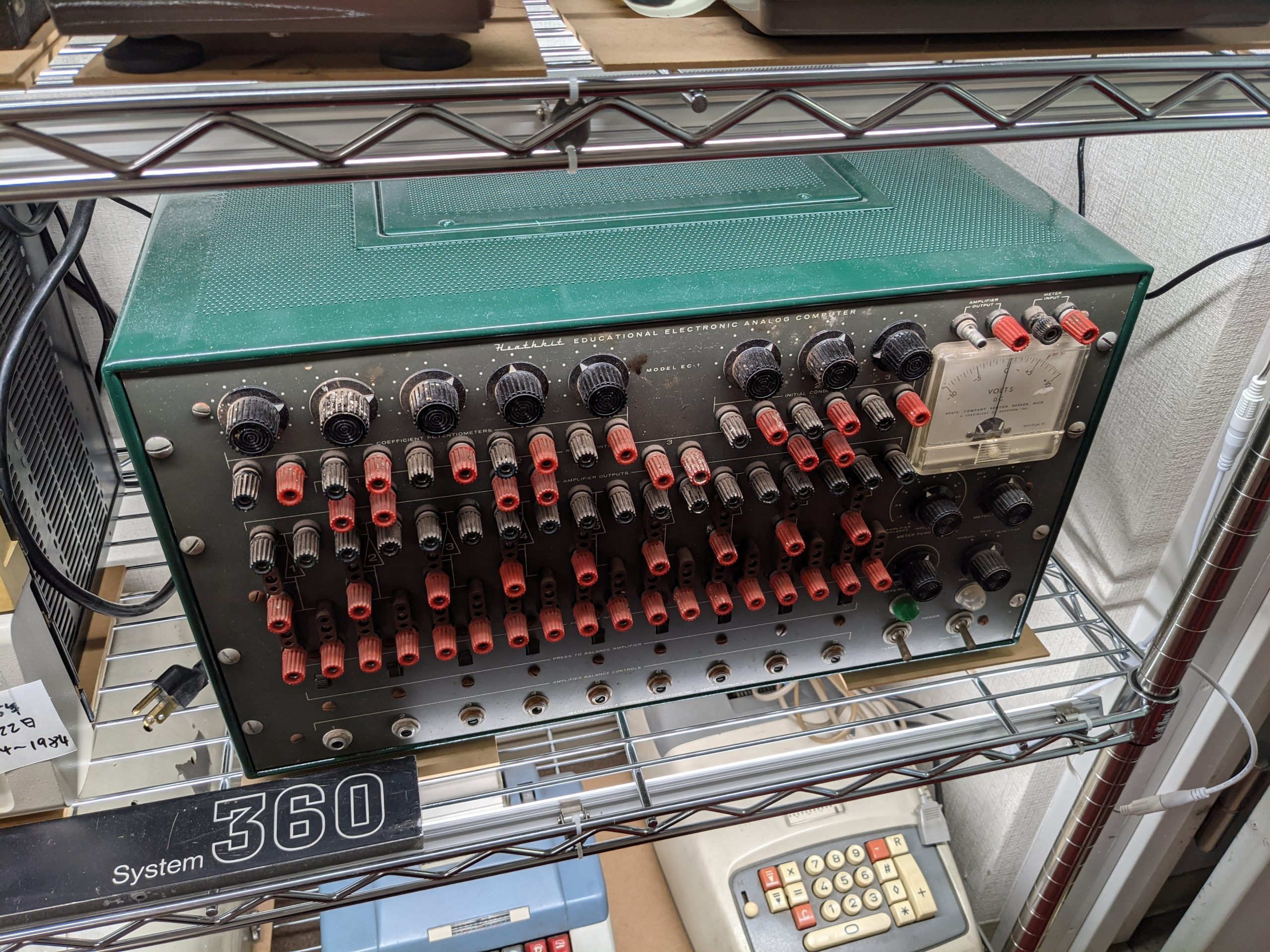
Heathkit EC-1 manual (PDF) (this manual itself lists a lot of references to books from the 1950s, most of which seem to be available on archive.org! If you’re into that kind of thing.) It looks like this manual already contains a bouncing ball circuit; a lot of people seem to be under the impression that Telefunken were the first to have such a circuit in their manual.
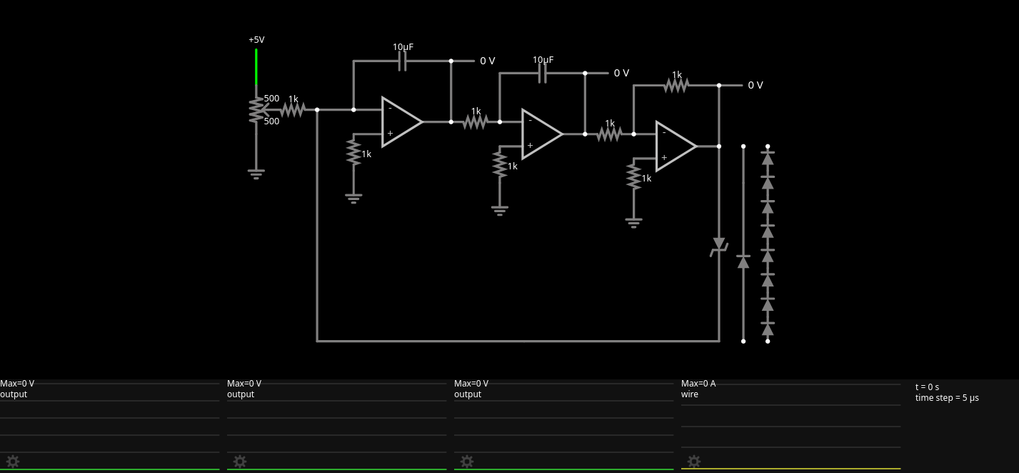
Analog computers were a thing, a long time ago. What do they do? They basically consist of a power supply, a breadboard-like area, a bunch of potentiometers to set input values, and a bunch of op amps in various configurations. The breadboard-like area would (for example) be color-coded and the user would attach jumper cables between different color-coded areas. However, back in the day, op amps weren’t tiny ICs that could be had for the price of a paper airplane folded out of old newspaper. They were discrete, and made of vacuum tubes (when they were invented in 1941), or, after transistors became available, discrete transistors.
Using analog computers (and op amps), you could, for example, sum voltages, invert voltages, and integrate and differentiate voltages over time. Let’s try and remember some calculus from high school or university and recall what differentiating and integrating means.
If you don’t have any basic knowledge of op amps yet, EEVBlog has a good video explaining the basics at https://www.youtube.com/watch?v=7FYHt5XviKc. It isn’t absolutely necessary to understand the basic concepts of op amps, you can just use them as “black box” integrators.
Some math
If you don’t remember much with regards to differentiation and integration, skip to the next paragraph. If you remember a bit more, here’s the ultra-condensed version of the below explanation: Differentiating a curve gets us a straight line, differentiating a straight line gets us a constant. Integration is the opposite of differentiation, so disregarding some lossy bits, integrating the constant gets us the straight line again. Integrating the straight line gets us the curve again. We can easily set a constant voltage using a potentiometer, and we can easily integrate using op amps.
Now, the less condensed version: here is a random list of facts that you may or may not remember:
Integrating is the opposite of differentiation (that’s the easy one)
Differentiation means getting the slope of a curve
Integration, being the opposite of differentiation, means that we get the curve from the slope (a slightly lossy operation, as there is more than one curve with the same slope)
You can differentiate things more than once. For example, from a quadratic curve (e.g., f(x)=x²) the first derivative yields a straight line (f'(x)=2x), from the straight line you get a constant (f”(x)=2). Integrating can be done more than once too, and as mentioned before, is the other way round, so from a constant you get a straight line, from the straight line you get a quadratic curve.
Now let’s say we have some acceleration, like… for example 9.8 m/s². (There is a planet called Earth in the Milky Way, named after the fact that some of its crust consists of earth. The same type of earth as you’d find in a potted plant. When you drop objects from a small height onto this planet, they accelerate, and the rate of acceleration is 9.8 m/s². 9.8 is very close to π² and this is not a coincidence. Also the people who live there are made of meat, but that’s a topic for another day.) So after 1 second the dropped object has a speed of 9.8 m/s, and after two seconds it’s 19.6 m/s, etc. Dropped objects get faster and faster. If you plot the speed of the object, you get a linear (i.e. straight) graph. However, if you plot the distance of the object from the point it was dropped, you get a curve, i.e., it gets steeper and steeper.
Let’s say, all we have at first is a constant, 9.8. In math terms, we could say that the function always producing this constant is f”(x)=9.8. (I added two apostrophes to “foreshadow” that we will be integrating this twice.) To get a linear function from the constant, we can integrate. The mathematical result of the integration is f'(x)=9.8x (+ some constant, which we will ignore here and below). Don’t remember enough about this to believe me? Try https://www.wolframalpha.com/input?i=integrate+9.8
This would draw a line with a rather steep gradient of 9.8. Implemented using op amps, the integrating op amp will have 9.8V on the input side, and a voltage linearly going up on the output. (Note: the op amp will invert the input, so in reality the voltage will go down, but that is not a major problem.)
To get a function that would plot as a curve from this linear function, we integrate again using a second op amp, and the result will be the function f(x)=4.9x² (ask Wolfram Alpha if you don’t remember how to do this (“integrate 9.8x”)). Now check out the formula to get the distance fallen after a time of t seconds at https://en.wikipedia.org/wiki/Equations_for_a_falling_body#Equations:
Hey, that’s exactly the same formula! (g is 9.8, 1/2*g is 4.9, and t is just a rename of x.)
(Done with the math, time to talk about some electronics)
On an oscilloscope, the Y axis is voltage and the X axis is just “time”. Oscilloscopes commonly offer another mode, the X-Y mode. In this mode, one channel’s voltage will be plotted on the X axis, and another channel’s voltage on the Y-axis. Using this mode, we can simulate the effects of gravity on the Y axis and the horizontal movement of a tennis ball on the X axis. (Of course, the X-Y mode won’t exactly make it easy to debug things, so for now we’ll mostly work in the regular mode.)
Just a few more notes and we’re ready to implement stuff on breadboards and start looking at the resulting signals on an oscilloscope!
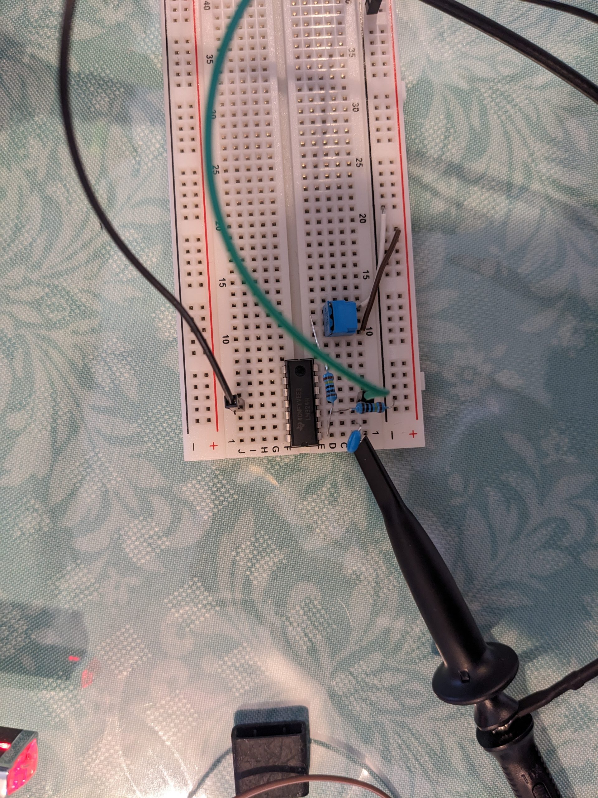
The power supply needs to generate a negative voltage, 0V, and a positive voltage. I’m using an old ATX power supply that I bought at a thrift store and have -5V/5V as well as -12V/12V. I use -5/5V below, this makes it much easier to interface with other components. If you don’t have anything fancy, you can just use two 5V wall warts back-to-back, or a couple AA batteries in series and tapped in the middle, or whatever you want!
Constants are just arbitrary voltages input using potentiometers. We don’t have to use 9.8V, we’ll just use something that is convenient and looks okay.
To integrate an input signal using an op amp, all we need to do is put a capacitor between the input and the output of the op amp. We’ll also need a resistor to make the integration happen non-instantaneously. (Check https://en.wikipedia.org/wiki/Op_amp_integrator or similar to learn more)
The op amp’s output will be inverted
To make the integration slow enough, we need capacitors with a high capacitance. But preferably we don’t want to have to take capacitor polarization into account, so we won’t use electrolytic capacitors. I’ll be using a 1 μF ceramic capacitor, which is the highest non-polarized capacitor value I have and makes our calculations very easy. We’ll also need resistors with a high resistance in the MΩ range, as the RC delay when using a 1 MΩ resistor with a 1 μF capacitor is 1 second (1000000 x 0.000001 = 1).
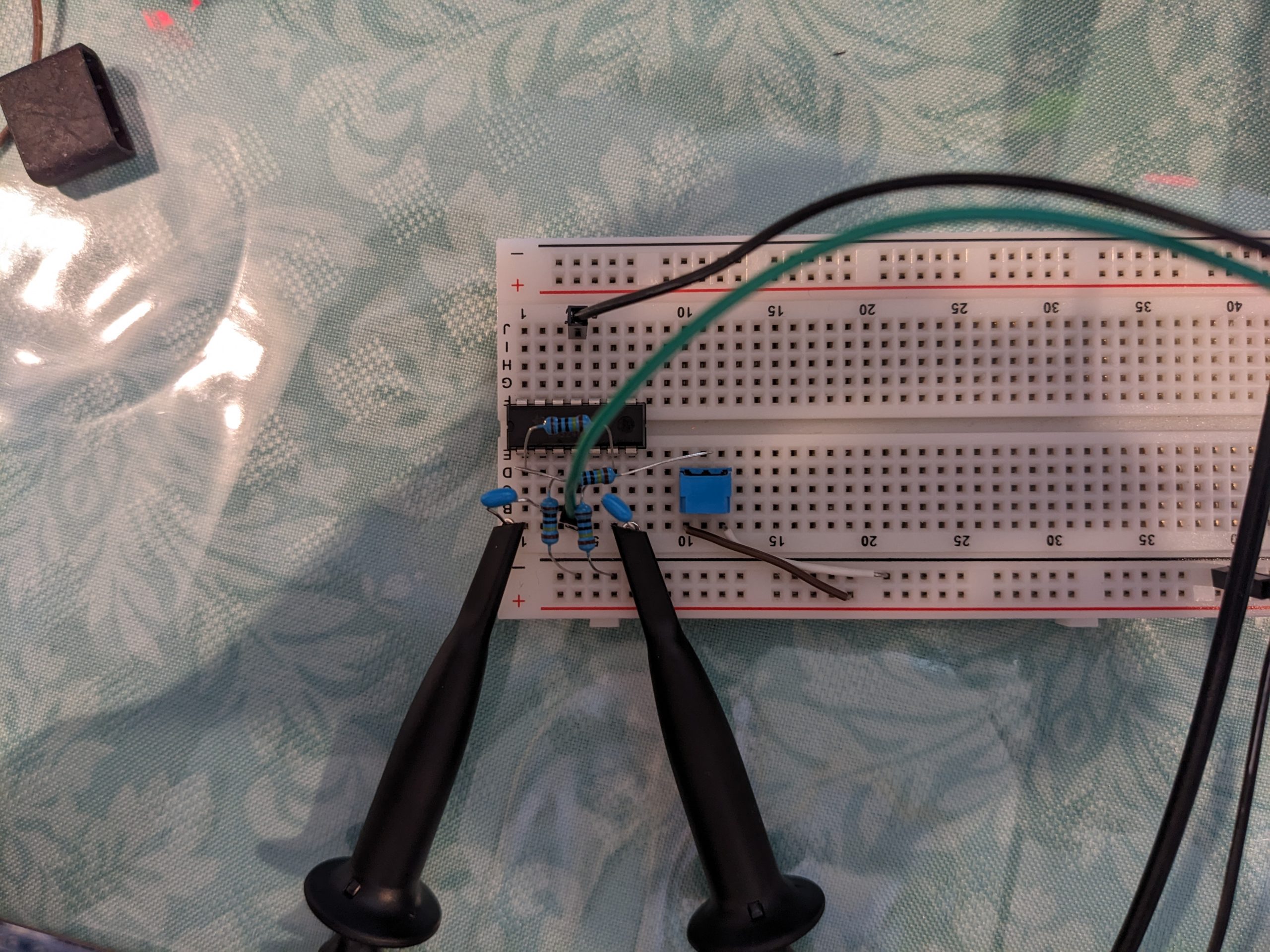
To get started, here’s the setup with an op amp integrating our constant fed in using a potentiometer:
The wire on the left side goes to -5V (or -12V; currently I’m using -5V and 5V rails because that’s more compatible with the components I have on hand). The breadboard voltage rails are 5V (red) and GND (black).
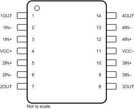
In this circuit, I’m using an LM324N quad op amp. The pinout looks like this:
(Note that the IC’s rotation isn’t the same in the above two pictures)
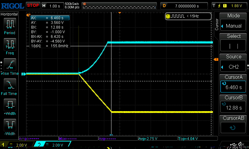
And here’s what we get on our oscilloscope:
Wow such straight lines!
Let’s integrate that straight line again. Here’s our setup:
And here’s what we see on the oscilloscope (probing the previous output stage and this output stage at the same time):
Is that all there is to the Y axis? Well, no. First of all, we are currently falling “up”. That’s easily fixed; we could just invert the signal again using another op amp. Or maybe we could simply input a negative voltage as our gravity, then we wouldn’t need to use an extra op amp circuit? Let’s not worry about that for now, we have some other things to take care of. Remember, this game/simulation is supposed to be tennis-like.
Tennis balls should bounce off the floor. Oh right, we don’t even have a “floor” yet, per se. We see that both signals reach “a floor” or “ceiling”, but they’re actually just reaching the op amp’s voltage rails (-5V and 5V) or the voltage set by the potentiometer, at which point they can’t go any further.
To make the ball bounce, we can “override” the gravity input and quickly feed in a negative voltage instead. (Of course, the gravity input is still there, just with a much higher resistance.) Conveniently, our floor is a negative voltage. (In the above pic, we’re still inverted of course. If we add another op amp, we can invert this signal.) We just need to “copy” this voltage to the – input of the very first op amp and we’ll produce a beautiful bounce. (“Cool so we just write some code and copy some variables, right.” “Wrong, sit down!”)
One immensely popular way to copy a voltage from one place to another is to use a wire to connect the two places! But in our case, we want a smart wire. This wire shouldn’t be active until we reach the floor (which is just a certain negative voltage of our choosing). Well, it may not be immediately obvious, but one of the most famous components in the world of electronics happens to have this property! We have surely heard of diodes before, right? A single standard diode doesn’t become active until we reach 0.7 V. If we use two diodes, it’s 1.4V, three diodes, 2.1V, etc. If we have negative voltages, we just flip the diode’s terminals around. Cool! But inconvenient. Here’s another type of diode though: the zener diode. Zener diodes are designed to be reverse-biased and become conductive (generally, very suddenly) at a certain voltage. So instead of (e.g.) stacking four regular diodes, we could use a single zener diode with a breakdown voltage of approximately 2.8V (and flip its poles because it’s reverse-biased).
So we just connect the output of the third op amp back to the input of the first op amp, via a diode!
Here’s a simulation of this circuit. (Note 1: this circuit uses wildly different resistor/capacitor values from the ones we were using before; note 2: please press reset first) The third scope is the y output of this circuit. Feel free to experiment by taking out the zener diode at the right and plugging in the single diode (which is a hypothetical diode with a forward voltage of 10V or so) or series of (normal) diodes instead. Note that directly connecting a negative voltage to a place that already has a positive voltage will produce a large current. This current is visible in the fourth scope in the simulation.
Well, things don’t look too bad in this simulation! Currently, the ball just bounces back to its previous level, but we could easily add a little something to dampen the voltage, which I may or may not explain later:
Look at the third scope, that looks quite like what we are after, does it not?
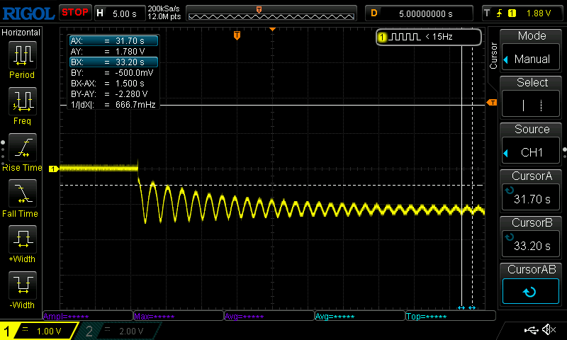
Well, things don’t always play out the same in the real world. Here’s the output of the circuit without any damping applied. As we can see, there is some damping anyway. Furthermore, the floor voltage level moves up over time, which is something I hadn’t expected.
So instead of using a zener diode to set the floor, we might want to explore some other options.
Use an ideal diode or ideal zener diode.
Use some other type of diode.
Use a comparator to compare against a configurable floor voltage level.
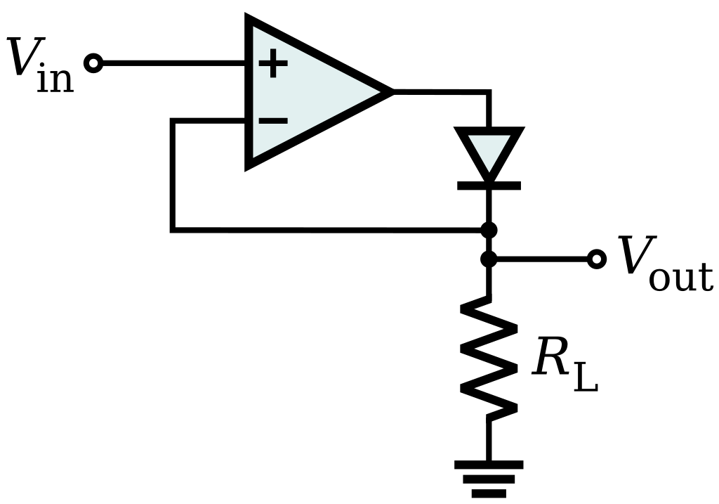
Oh yeah, an ideal diode! Silly me, messing around with them non-ideal diodes. Let’s pay a couple cents more and buy some ideal ones, right?!
Enter the precision rectifier
Above, we described diodes and zener diodes as “smart wires” that become active at a certain voltage level. But that’s an “ELI5” explanation. Diodes are actually kind of devious; they do become active at a certain voltage, but when they do, they substract that voltage from the input voltage!
This sort of behaves like an ideal diode!And this one is even more ideal because I hear this one can be used with negative voltages.
These circuits behave like diodes that don’t have a voltage drop. な、何!? Op amps, is there any thing they can’t do? There are versions that do full wave rectification too.
By the way, we find something close to the basic version of the precision rectifier in Mubarik Mohamoud’s circuit (page 7 of the PDF):
To be honest, using these things won’t help us much on our quest to keep things simple. We don’t need a perfect circuit; let’s use some artistic license and check out some other diodes first!
Other diodes
There are other diodes out there that have a high forward voltage. For example, how about… a white LED?!
Using a white LED between the output of op amp 3 and input of op amp 1, we get automatic damping… and actually this looks pretty damn good, you’re hired!The LED blinks every time we reach its forward voltage. Kinda cool IMO! (Don’t stare too hard at the breadboard, it’s not in a clean state right now. Or the dangling jumper wire, which looks pretty close to shorting something to GND ^_^)
Of course, if we wanted to be exact and stuff, we should maybe look into using comparators instead! We’ll definitely need comparators at some point so why not check them out now.
Enter the comparator
We could also use a comparator, and yes, you guessed it, our good old omnipotent friend Op Amp can be used as a comparator, because of course he (or she) can! We’ll make an op amp compare our Y coordinate voltage with a low voltage set using a potentiometer. That’s our floor.
Op amps used as comparators always output their low voltage rail or their high voltage rail, depending on whether the input voltage is lower or higher than the reference voltage. Our above op amp had 5V and -5V rails, so the comparator would output 5V or -5V. -5V is not convenient for what we’ll do later, so we’ll convert -5V to 0V by feeding the output to a diode. The negative voltage won’t make it through, only the positive 5V. Because the negative voltage won’t make it through, it will be like the input is floating. We will add a pull-down resistor.
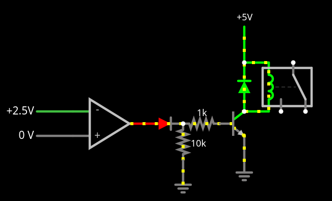
To make our comparators actually do stuff, we can use relays. (We could use many other things, the most simple/convenient of which might be a CD4016 or similar, but the original Tennis for Two used relays, so we will too!)
How do we connect our relay to an op amp output? Well, op amps don’t like to drive heavy loads, so we’ll use a transistor (commonly, S8050 or 2N2222), like in the following circuit. (I’m not sure if the op amps of old were able to drive relays.)
This first diode keeps away the negative voltage. I also added a pull-down to ground, because otherwise the input would be floating. E.g., on my multimeter it reads as 2V. No 0V! No, 3V! The diode in parallel with the relay is to take care of back EMF from the relay.
We’d like the ball to do something when the player presses a button. In the original(?) game (https://www.youtube.com/watch?v=s2E9iSQfGdg), the ball is able to bounce off the net in the middle, and can be hit at a configurable angle. I’d say we skip the net for now, but we should implement the button. More on that later!
For now, let’s just quickly think about what we need to make happen when a player hits the ball.
The “gravity capacitor” keeps doing its thing at all times
We just want to momentarily input a higher voltage into the first op amp’s input
This voltage can be controlled using a potentiometer
We’ll talk about these potentiometers and buttons later.
The X axis
In a nice “Tennis for Two” game, players have beautiful controllers that have a button. This button changes the current direction of the ball. (Let’s define that a little more precisely: player 1 can only invert the direction of a ball flying right-to-left, and player 2 can only invert the direction of a ball flying left-to-right.)
In addition, there should be some kind of potentiometer inside the controller, allowing players to hit the ball hard or less hard.
Before we dream of making an ergonomic controller (yes yes, it should incorporate glass and steel and Nixie tubes to display the current score), let’s think about what the X axis is even supposed to look like.
The “distance traveled” plot for the Y axis was a curve, but for the X axis, it’s a straight line. Conversely, the “velocity” plot for the Y axis was linear, but for the X axis, it’s a constant. (For illustration: in the plots below, the ball travels at a constant velocity of x volts/second.) (In reality the X axis velocity should slow down a little bit over time due to air resistance; we could model this by fudging in some kind of damping mechanism.)
The X axis circuit works like the Y axis circuit, in that it is built from op amps. However, we integrate only once. (So just a single op amp, actually.) In the Y axis, we integrated twice. (See above if you can’t remember how that worked.)
First of all, some definitions: player 1 is on the left side of the screen (where the X axis is negative), player 2 on the right side (where the X axis is positive). Here are some example graphs of the X axis:
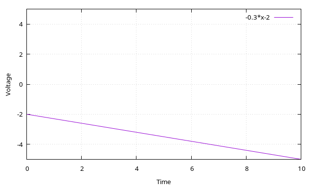
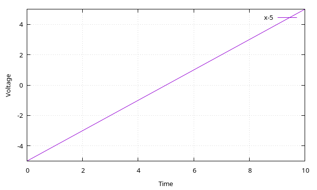
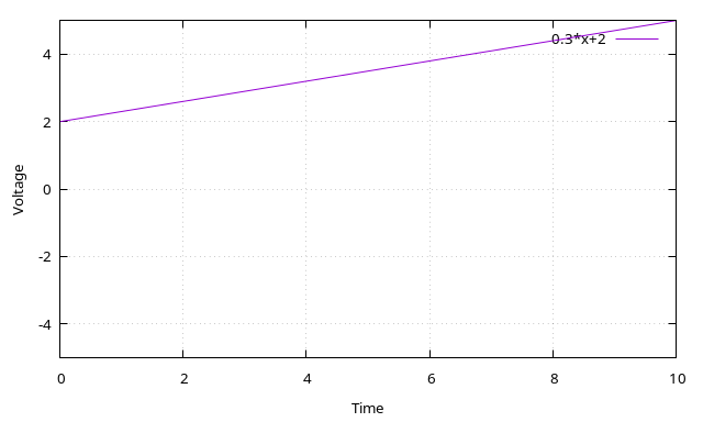
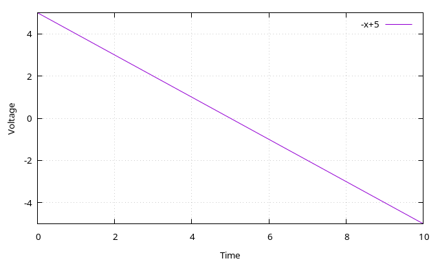
A negative voltage that is going down: ball is in left side of screen and moving farther left. Player 1 can hit the ball in this state. Player 2 can’t. Velocity is -0.3V/s.A negative voltage that is going up (like in the above picture): ball is in left side of screen and moving right. Player 1 can’t hit the ball in this state. (Most likely they already hit the ball.) Player 2 can’t hit it either. After we cross 0V (at the 5 second mark), player 2 can hit the ball, player 1 can’t. Velocity is 1V/s.A positive voltage that is going up: ball is in right side of screen and moving right. Player 2 can hit the ball. Player 1 can’t. Velocity is 0.3V/s.A positive voltage that is going down: ball is in right side of screen and moving left. Player 2 can’t hit the ball in this state (they probably already did). Player 1 can’t hit it either. (Once the voltage crosses 0V (at the 5 second mark in this graph) and goes negative, player 1 can hit the ball.) Velocity is -1V/s.
Players use a potentiometer to decide how hard the ball is hit. This potentiometer sets a voltage that represents the velocity. This voltage is connected to op amp 1.
Here’s an example of the ball being hit:
Here player 2 (positive voltage, so on the right side) hits the ball relatively softly at the 4 second mark and the ball changes its direction.
(Hey, gnuplot, it’s been a while.)
There is one minor engineering problem: as the player sets the velocity with their controller, we have to make sure they can’t change the velocity after hitting the ball. If we just hooked up the potentiometer directly to the first stage op amp, the player could/would make the ball slower or faster in mid-air by fiddling with their potentiometer after hitting the ball. Not very tennis-like!
How can we do this? Well, there should be a momentary push button. If this button is pushed, there should be a check to see if we are on the correct half of the screen, and if the ball is traveling in the correct direction. This is implemented using comparators and AND circuits. If the checks pass, we apply the voltage set by the potentiometer to feed op amp 1.
We need to check conditions. We use op amps configured as comparators. We could easily use NPN transistors to form an AND gate but we’re lazy and will use 74-series AND logic chips. (Which weren’t quite around yet when this game was invented!)
Our comparators compare against the middle of the screen, which is 0V. This makes the wiring very easy: one input is the current voltage, and the other input is GND.
The other player has the inputs on the comparators swapped. (I.e., “one input is GND, the other input is the current voltage”)
One voltage is the current voltage as it is output by the X axis op amp (the absolute position of the ball on the screen), the other voltage is the voltage that is input into the op amp (i.e., the output of the sample and hold circuit mentioned below).
After checking the conditions, the new voltage is set. This immediately changes the ball’s direction, which means that the conditions are no longer true after a very short moment.
However, we need to keep applying the same voltage until the other player presses their button.
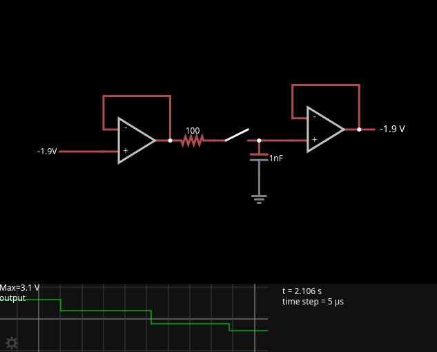
We can store the potentiometer voltage in a sample and hold circuit.
Sample and hold circuit
Well, apparently there are many ways to build a sample and hold circuit. I happen to have a (Japanese) book called 回路の素 101 that has a whole bunch of analog circuits, many of them using op amps, and among those, two circuits to do sample and hold.
If you like reading Japanese text, I recommend this book. I read it cover-to-cover a couple years back. I certainly don’t remember everything, and it doesn’t always explain everything, but I did (e.g.) remember reading about the precision rectifier (mentioned above) and that there was something similar to the hold and sample circuit.
Here are the two circuits in a simulator:
The (very) simple version (link to falstad simulation), circuit 53 in the book. (I’m using a different capacitor value.)
We can see that this circuit only holds the sampled value for a few milliseconds. The charging of the capacitor is slow, and it discharges itself pretty quickly.
The advanced version (link to falstad simulation), circuit 54 in the book. It holds the voltage rather nicely. The book uses a 220p capacitor.
In real life, I went for a 1 uF capacitor, for improved debuggability: when using an oscilloscope (or even multimeter) to make sure that your capacitor is holding the expected voltage, you will find that the voltage drops very quickly. This is due to the oscilloscope’s input impedance, which is likely 1 MΩ. Using a tiny capacitor, the voltage will be gone almost immediately. Using a 1 uF capacitor, you have a couple seconds.
“Controllers”
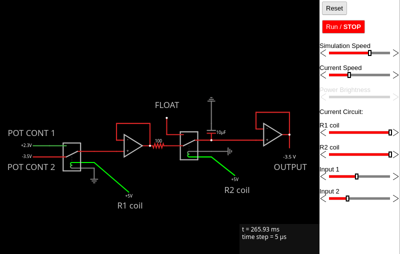
The controllers are conveniently placed on a hard to reach corner on the breadboard. We have two potentiometers and one button per player. When the button is pressed and the comparators’ outputs going to the AND chip look good, we drive an SPDT relay. SPDT means that the relay normally connects player 2’s potentiometer to the input of the sample and hold circuit. But when the relay is active, it instead connects player 1’s potentiometer to the input of the sample and hold circuit. (Or the other way round, it doesn’t matter much.)
The sample and hold circuit must hold a new value when either player 1 or player 2 presses their button (and the abovementioned conditions pass). This means that we need an OR circuit as well.
Outside the controller, we have a circuit that is inserted into the aforementioned sample and hold ciruit, as shown below. “Input 1” and “Input 2” are directly attached to the potentiometer outputs. The “R1 coil” (relay 1 coil) and “R2 coil” inputs are the binary signals mentioned above.
Here’s a schematic of this sub-circuit:
Circuit (Falstad simulation). AND circuit output is amplified using a transistor and goes to “R1 coil”. When this signal is 5V, the coil forces the relay to connect “POT CONT 1” to the output. When the signal is 0V “POT CONT 2” is connected. This goes into the input of our sample and hold circuit. The sample and hold circuit requires a switch in the middle. This switch is implemented using another relay that is controlled by the output of the OR circuit mentioned above. When the relay is off, it leaves the capacitor and op amp on the right floating. When the relay is turned on, we sample one of the potentiometers.
Other implementation notes
I used a 74LS08 chip for the AND gates. I’m using all four. I used a 74LS02 chip for the OR gate. This is a NOR chip, and I’m using two NOR gates to emulate one OR gate. The remaining two NOR gates are currently not used. These logic chips could be replaced with BJTs if you want to make the whole thing more era-appropriate, but you might find that the naive AND/OR gate implementations are a bit janky.
There is a lot of space between the “sample and hold” op amp and the “comparator” op amps. I added an op amp I didn’t need!
Putting it all together
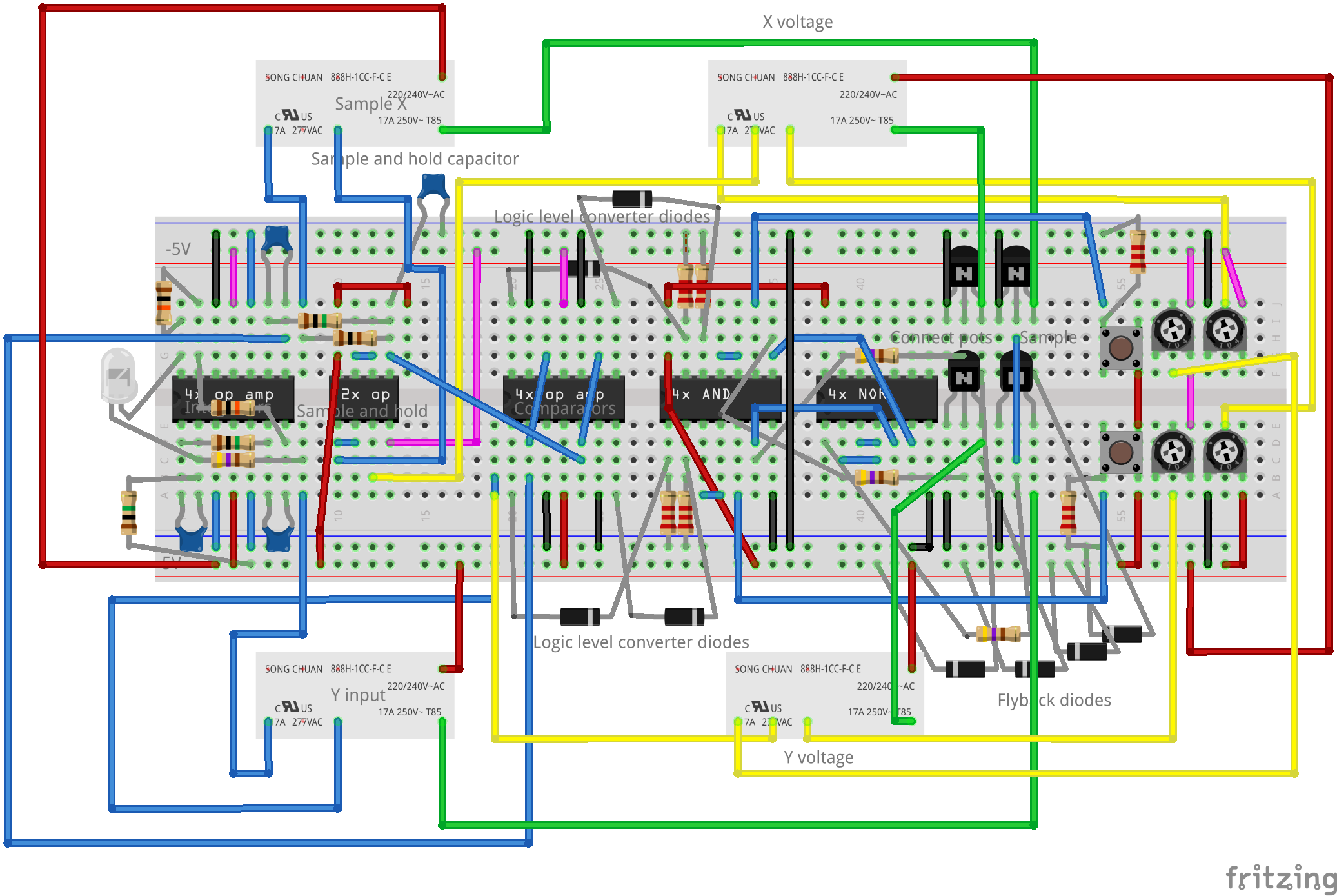
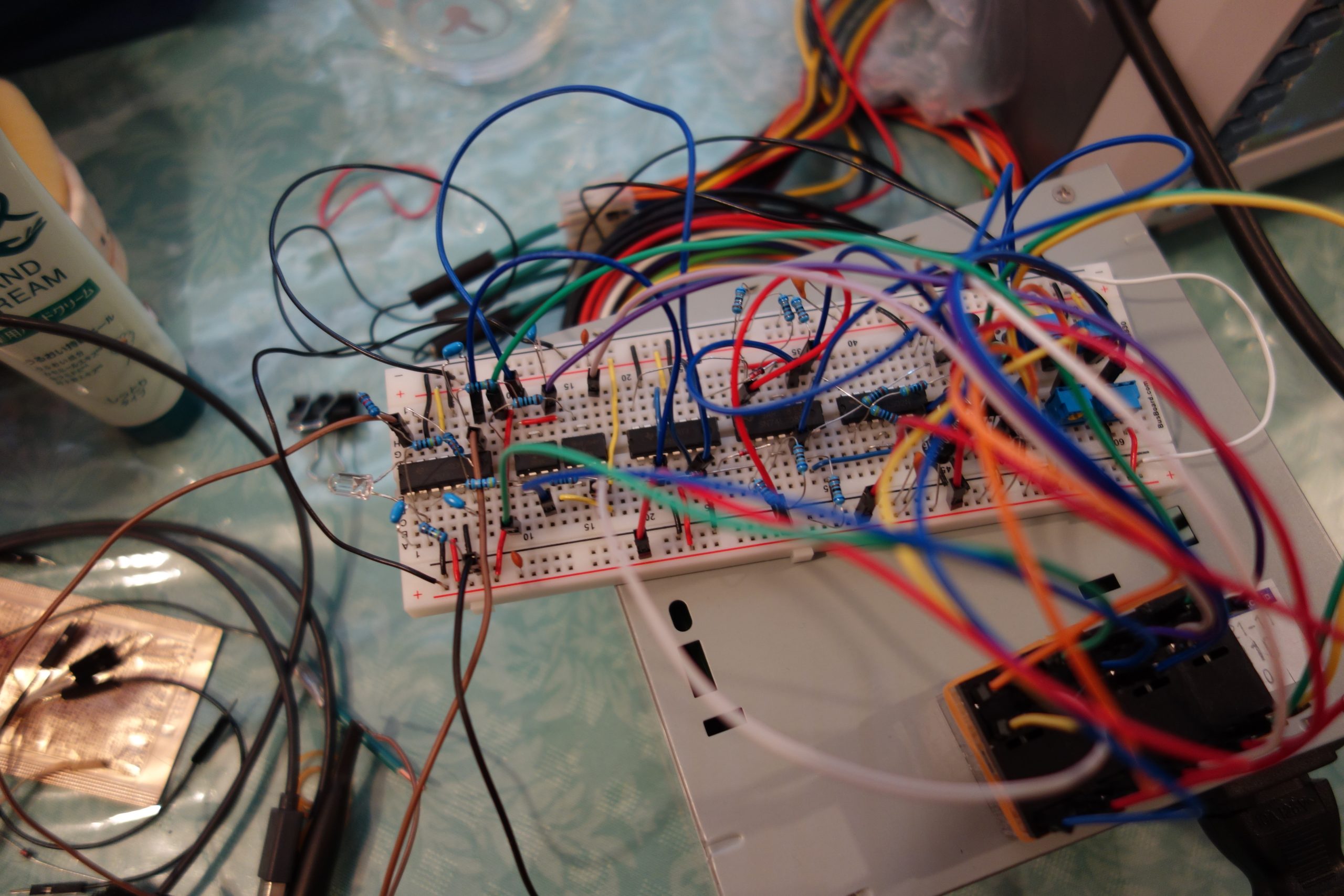
I decided to squeeze everything onto a single breadboard. To make this a little easier, I decided to build the circuit in Fritzing before building it in real life.
Change history: 2024-08-05 Initial upload (“v2”) Notes: The relays may not be connected correctly here — some things may not make sense (e.g. X and Y could be the wrong way round, or player 1’s potentiometer could be wired to player 2’s comparators, etc.) The relays shown in Fritzing (and thus the above image) aren’t the actual relays used. (Actual relays used are Omron G2R-1 5V relays. These don’t fit on breadboards, but we didn’t really have any space remaining on the breadboard anyway.) The real-life version (as seen in the picture/videos below) uses two dual op amps in the “sample and hold” region, though one is not required. There might be issues in this area. Red means a connection to +5V, purple means connection to -5V, black means connection to GND, green means connection from transistor to relay, yellow means connection from relay to somewhere on the breadboard, blue means “other connection” on the breadboard. I mostly tried to follow this rule when building the real thing, but 1) my connections from board to relay are random, 2) connections from power supply to board are all black, 3) the white wire sticking out to the right is GND and should be black. You don’t have to use LM324s and LM358s. It’s just that I had a bunch of these lying around, waiting to be used.
Pics/videos
In this video, I set the Y potentiometers to a rather low resistance. This causes the op amp’s capacitor to charge quickly. This means that the ball will be hit very high. Note: In the first shot, the ball goes above +4V, which is beyond the currently set voltage range (1V per division, oscilloscope is showing 4 divisions)In this video, I set player 1’s X potentiometer to hit the ball rather hard.
Taking things further
Here is a list of features that might be pleasant to have:
Proper controllers
A ceiling to bounce off of (I think this is just one extra diode). Should look better than a flat line when the ball hits the -5/+5V limits!
A nicer-looking ball
Some audio feedback (I thought the relays would provide this, but they’re relatively quiet, actually)
A net in the middle (both visually and functionally)
A way to detect if a player misses
Perform some game-like action when a player misses
A score counter
I think you’d need another breadboard to add all this!
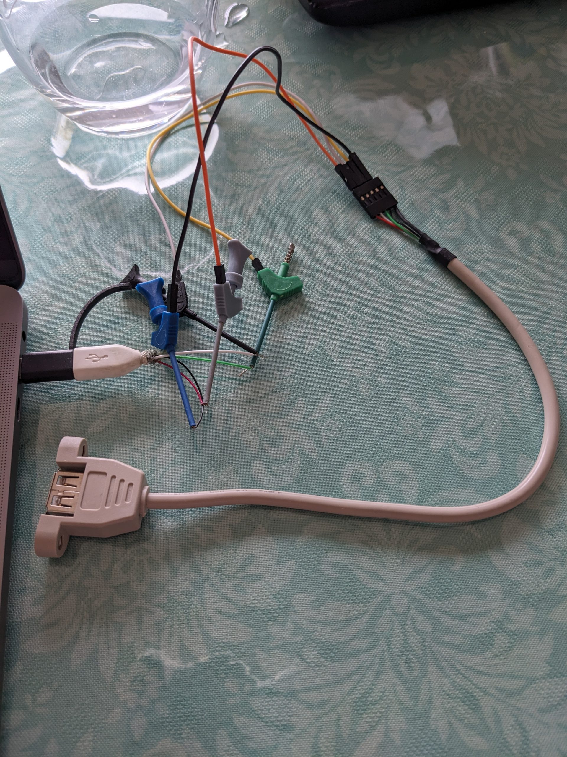
Argh, I hate laptops that don’t have USB-A ports. Especially today, as I forgot my adapters at the office. Again!
I happened to have a micro USB connector with exposed conductors. I happened to have a micro USB to USB-C adapter. I have a (non-janky!) USB port with Dupont connectors. One of my best purchases from Hard Off ever. And of course I have plenty of test clips.
(I’m actually supposed to have a USB-C connector with exposed conductors, I just did a couple months ago. But I just can’t find it. Maybe haven’t seen it since moving house.)
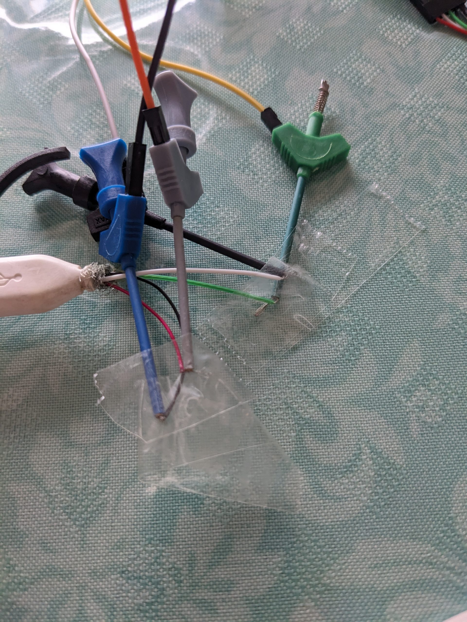
Let’s tape it down for electrical safety
And because the power wires on this connector look rather anemic I used a powered hub. A USB 1.1 hub, BTW. Not sure if this is too janky for the blazing speeds of USB 2.0. (Also a great purchase from Hard Off, BTW.) Microcontrollers like the RP2040 and ESP32S3 only support USB 1.1 so these things are useful again these days. E.g. USB (UVC) cameras set a different descriptor when connected via USB 1.1 vs. USB 2.0. Note: my particular hub wouldn’t work until I connected the VCC wire. I don’t think this is required for all hubs.
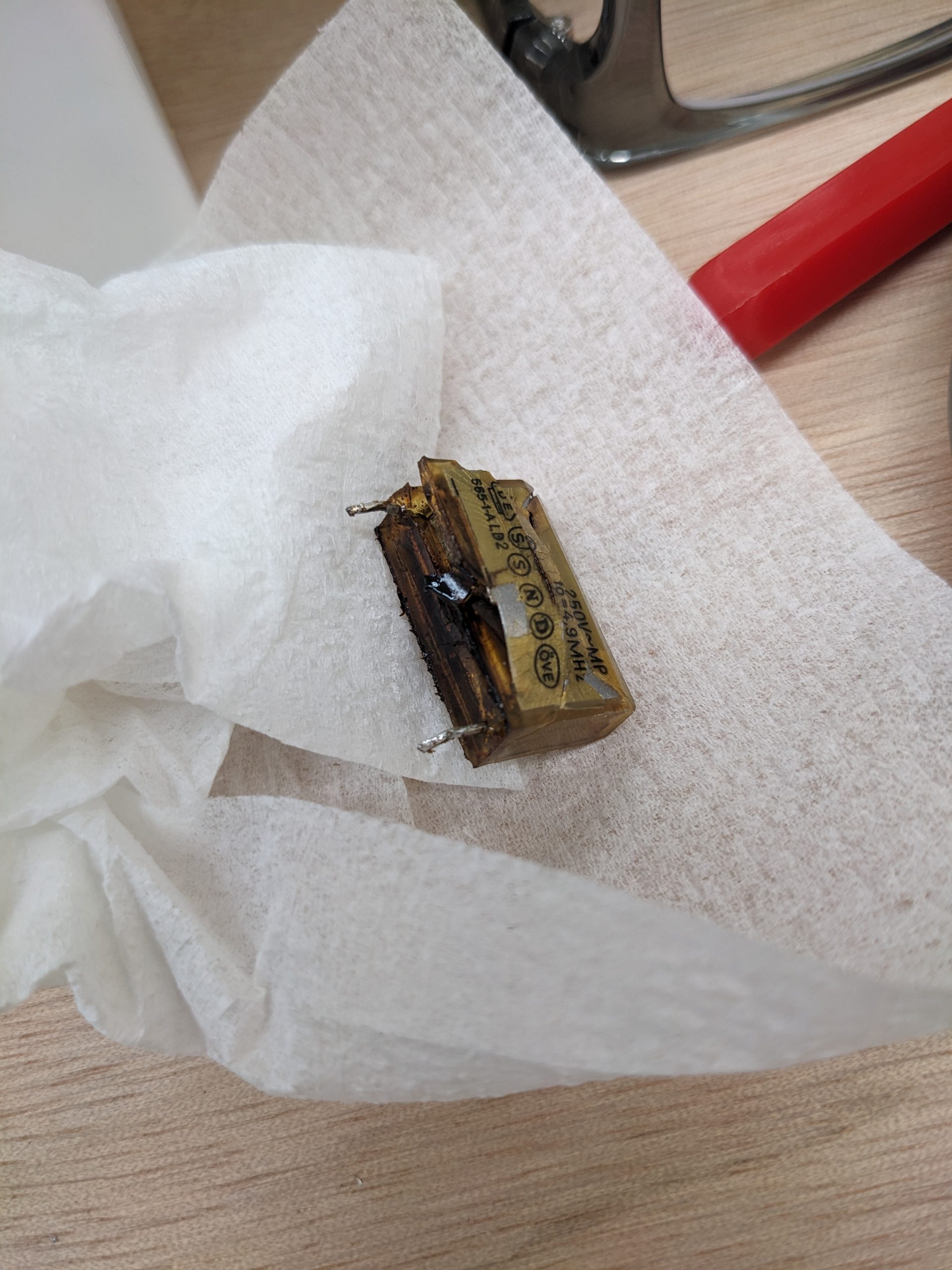
Well, I finally had a chance to see a few of those infamous RIFA metallized paper capacitors first hand!
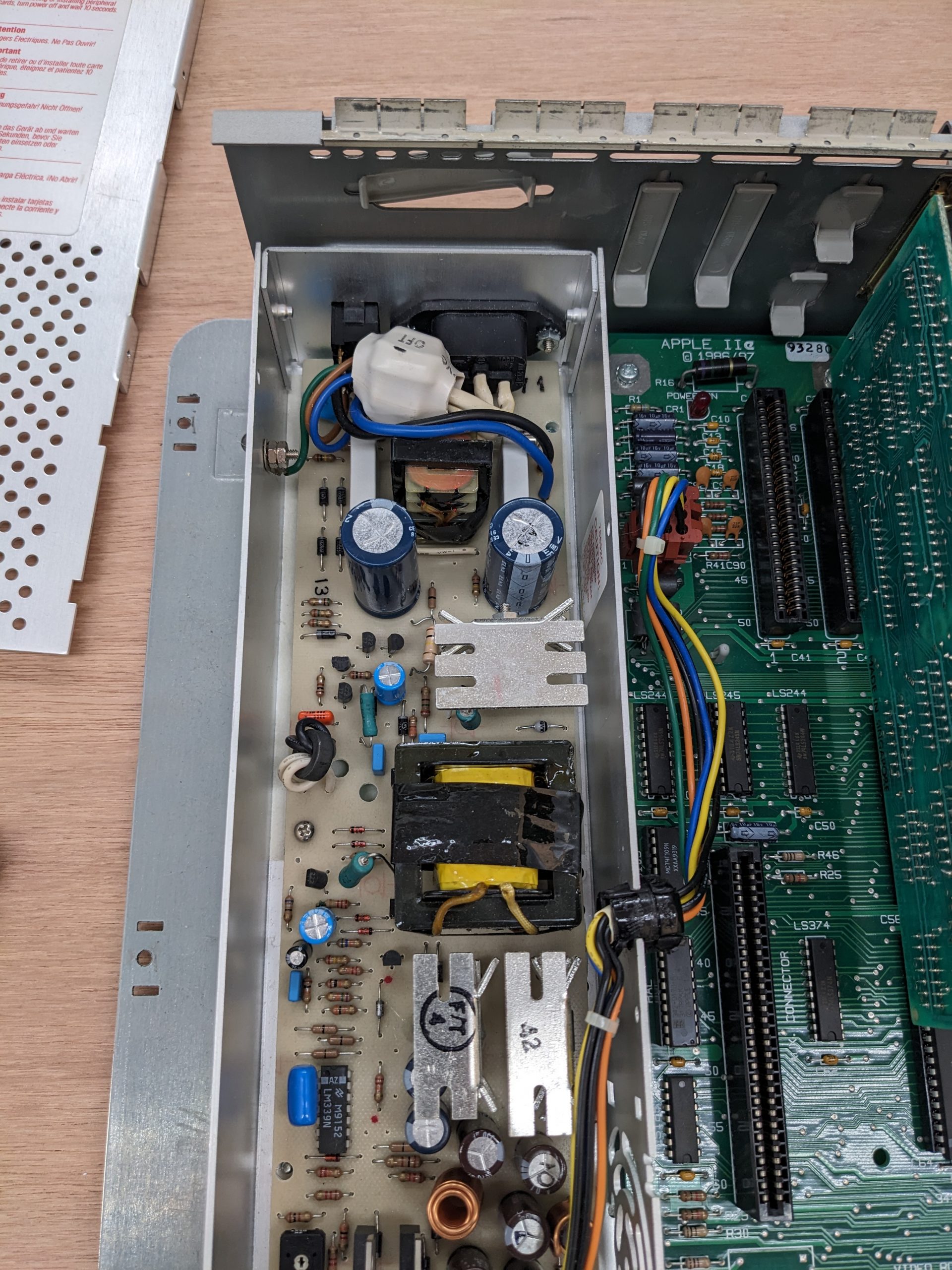
Yesterday, I had a look at two Apple IIe machines. One was from 1987. This computer works and is in really good condition and bears the signature of Steve Wozniak. I thought it would be a good idea to go and check for RIFA capacitors in there, but there weren’t any. Here’s a picture of its really clean power supply:
I am guessing that those two white things are the noise suppression caps.
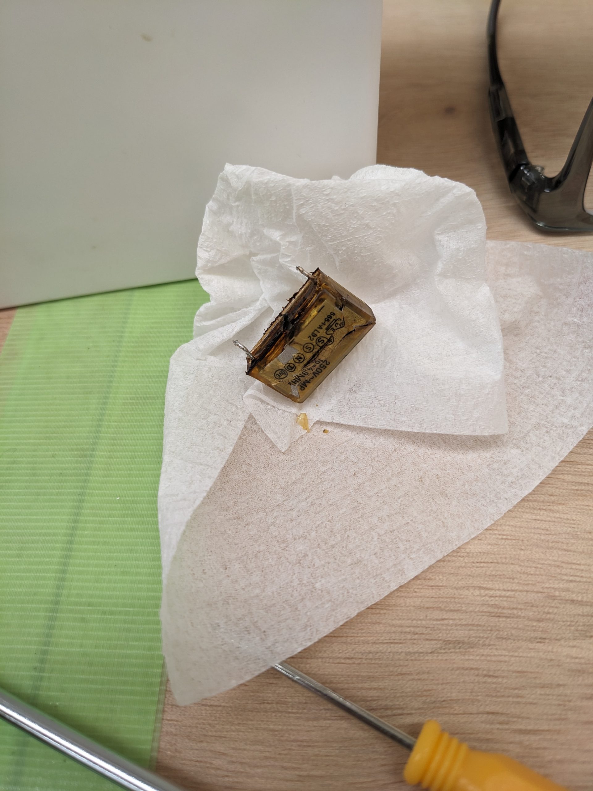
The other Apple IIe doesn’t work. The person running this machine immediately switched off the mains line when smoke started coming out of its power supply. That’s good! The capacitor didn’t go short, and the fuse was still intact. Maybe it even reduced the amount of smoke and brown juice sprayed about its perimeter.
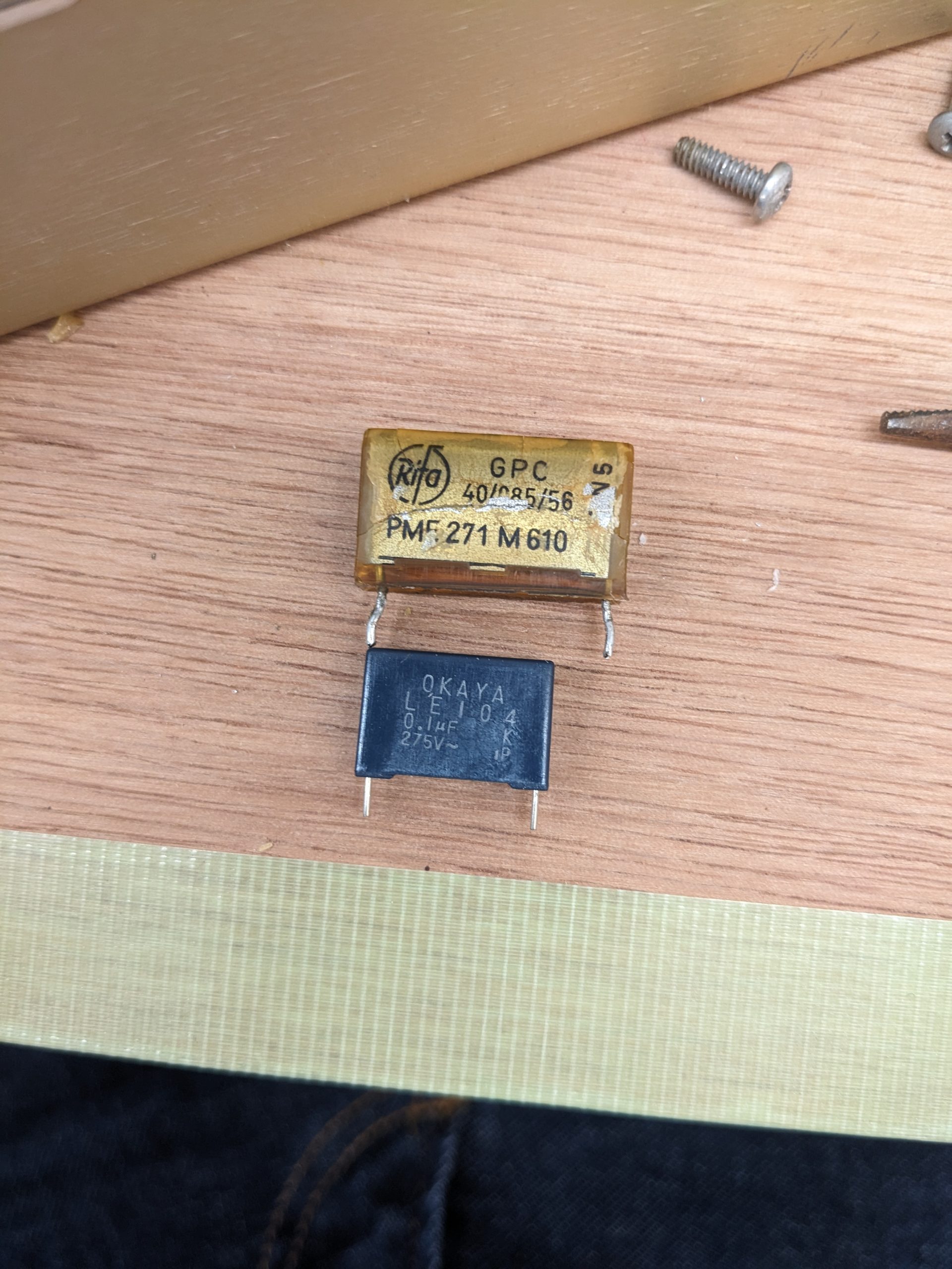
From the symptoms I’d correctly assumed that the owner had witnessed a RIFA capacitor explosion, so I came prepared by buying some replacement caps! I’d expected to have to bodge them due their size difference, but to my surprise, the PSU board had three holes for the noise suppression caps. The RIFA cap was using the outer holes (“holes 1 and 3”), and my smaller cap fit perfectly into holes 2 and 3! Cool beans.
Original RIFA cap (pin spacing of around 2 cm I believe) and replacement (1.5 cm). (The replacement cap has its X2-certification on the other side.)
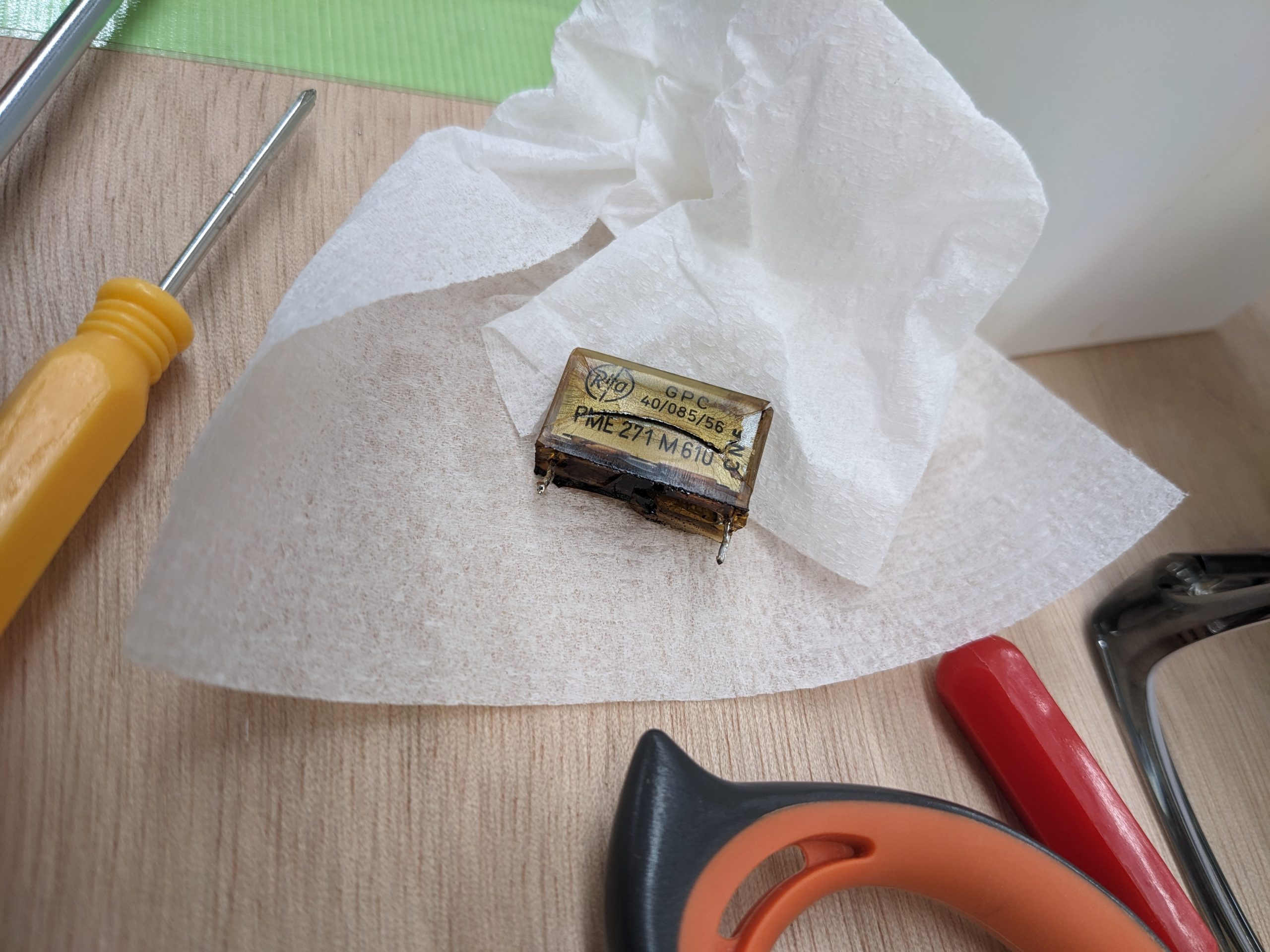
The PSU had two RIFA caps. The one pictured above is “intact”, though it has a huge crack in its plastic case. Here are the pictures that we’ve all been waiting for, the exploded cap:
The ejected brown juice wasn’t too bad and cleaned up quite nicely.
Here is the computer put back together again, already performing advanced calculations.
The end.
Edit 2024-07-11: one more, an Apple II Plus
This guy’s power supply was riveted. What the actual? I think the screws used were some tamper-proof kind, too. The rivets were drilled out and the screws still wouldn’t come out, beyond a millimeter or so. So the screws were drilled out too. It was a bit of a nightmare. The label on the power supply said Astec AA1040. There were no RIFA caps in it.
A while ago an acquaintance asked me to build a power supply for his replica Apple 1 board. He had all parts on hand (in fact, they were the exact parts mentioned in the Apple 1 documentation and schematics, Stancor P-380 and Stancor P-8667). My acquaintance probably knows a lot more than me, so I basically just did what he asked: I drilled holes into a sufficiently nice piece of wood from the 100-yen shop, soldered connections to the transformers (I believe they were probably salvaged, but luckily still had wires attached), added a fuse, soldered an AC cable into the mix, and soldered the Apple 1 power connector. Doing all this took between 4 and 8 hours, I don’t really remember. Here’s a picture of the assembled power supply.
With multimeters hooked up to each of the voltage rails (-12V, -5V, 5V, 12V), I hid behind a big rock and pushed down on an ACME plunger detonator. The explosion… didn’t take place, and the voltages were all good. Phew! Next I hooked up a period-correct monochrome CRT, and saw an image! A very jumpy image. It was possible to adjust HSYNC on the back of the CRT, which stabilized the image, but it still didn’t look correct. Pressing RESET or any other key on the keyboard didn’t do anything.
Stable (i.e., not rolling) but incorrect image
(Note on fuses: my fuse is on the primary side, mains voltage here is about 100V. I blew a 0.3A fuse on power up, then a 0.5A fuse on power up, and am currently using a 2.5A fuse. Maybe I’ll try 1.0A or 1.5A. Or maybe I should go and look at slow blow fuses.)
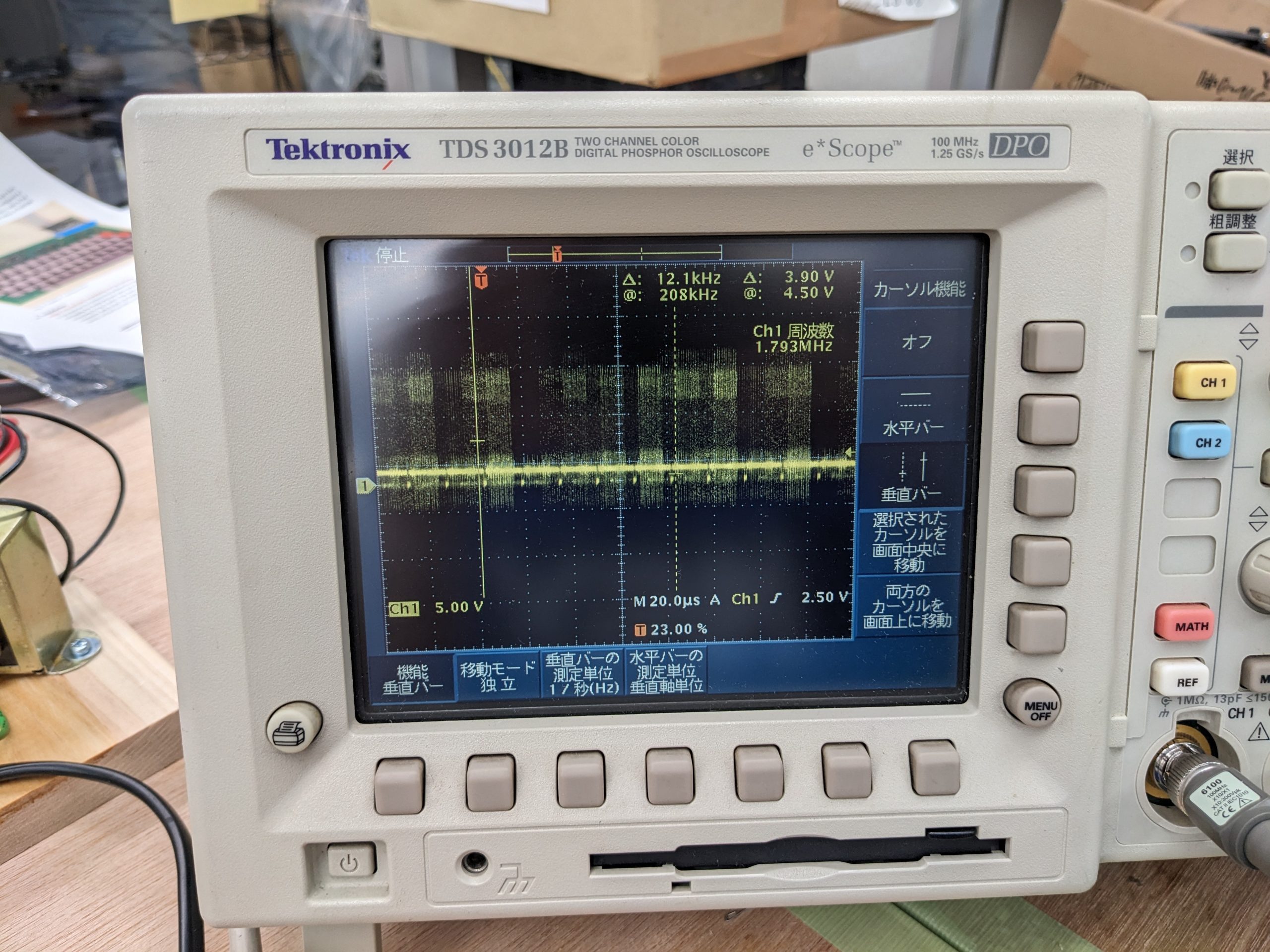
Before studying the schematics, I fired up an oscilloscope and had a look at the frequencies of the video signal. Here’s what I found:
Those small yellow blobs in regularly-spaced intervals close to the center line are the wannabe horizontal blank periods. They are supposed to have a frequency of 15.something KHz. In the above picture, I moved the oscilloscope’s vertical cursors further apart such that I get a frequency somewhat close to 15 (12.1 KHz), and as you can see we get 6 horizontal blanks in that period! This means the video signal is much too fast. I also looked for the vertical blank. It’s supposed to be 60 Hz and measured as 243 Hz. (Probably actually 240 Hz.) (At this point it’s worth worrying that we might be overclocking the CPU as well, but that wasn’t the case, it was running at a safe speed.)
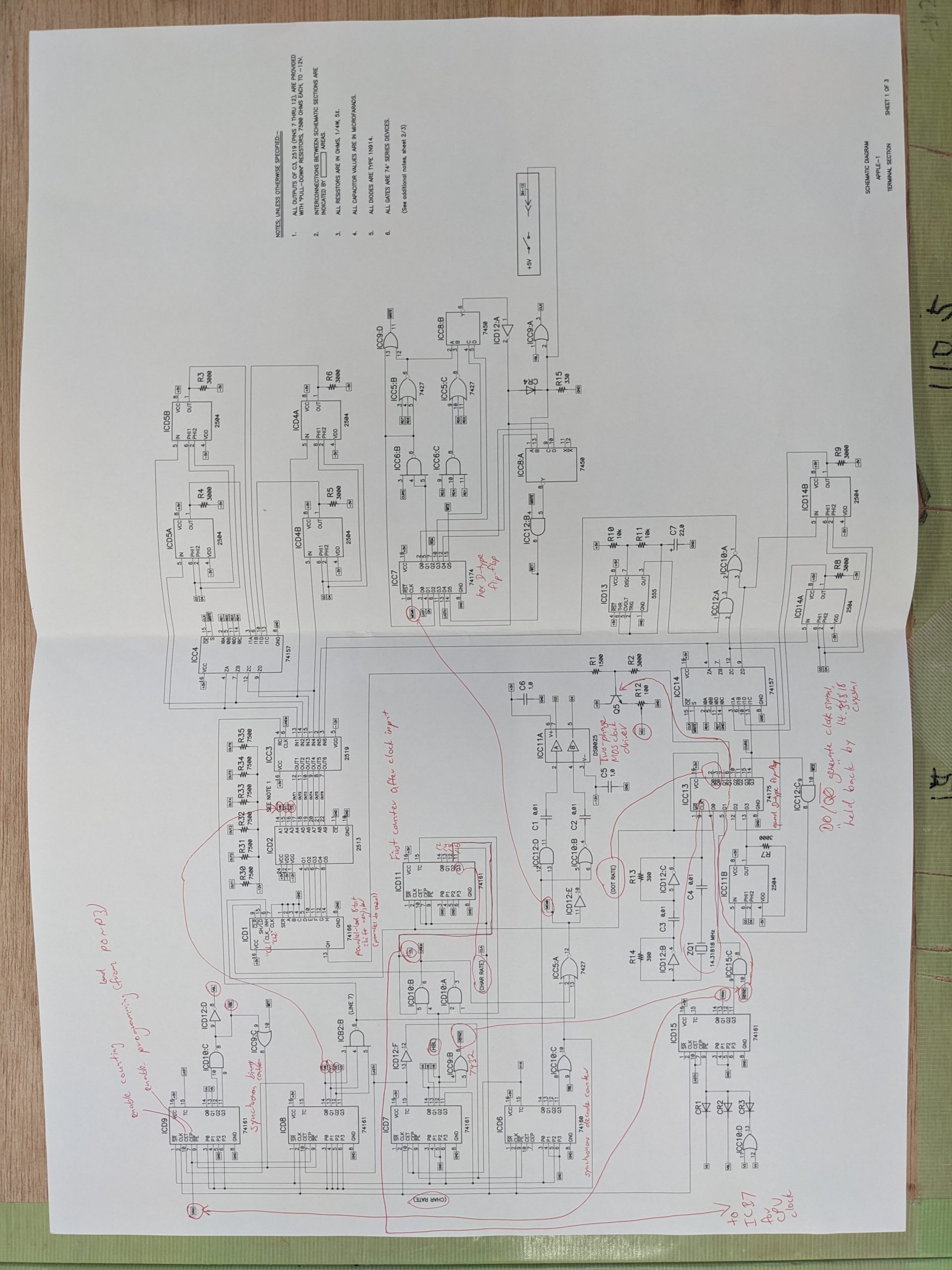
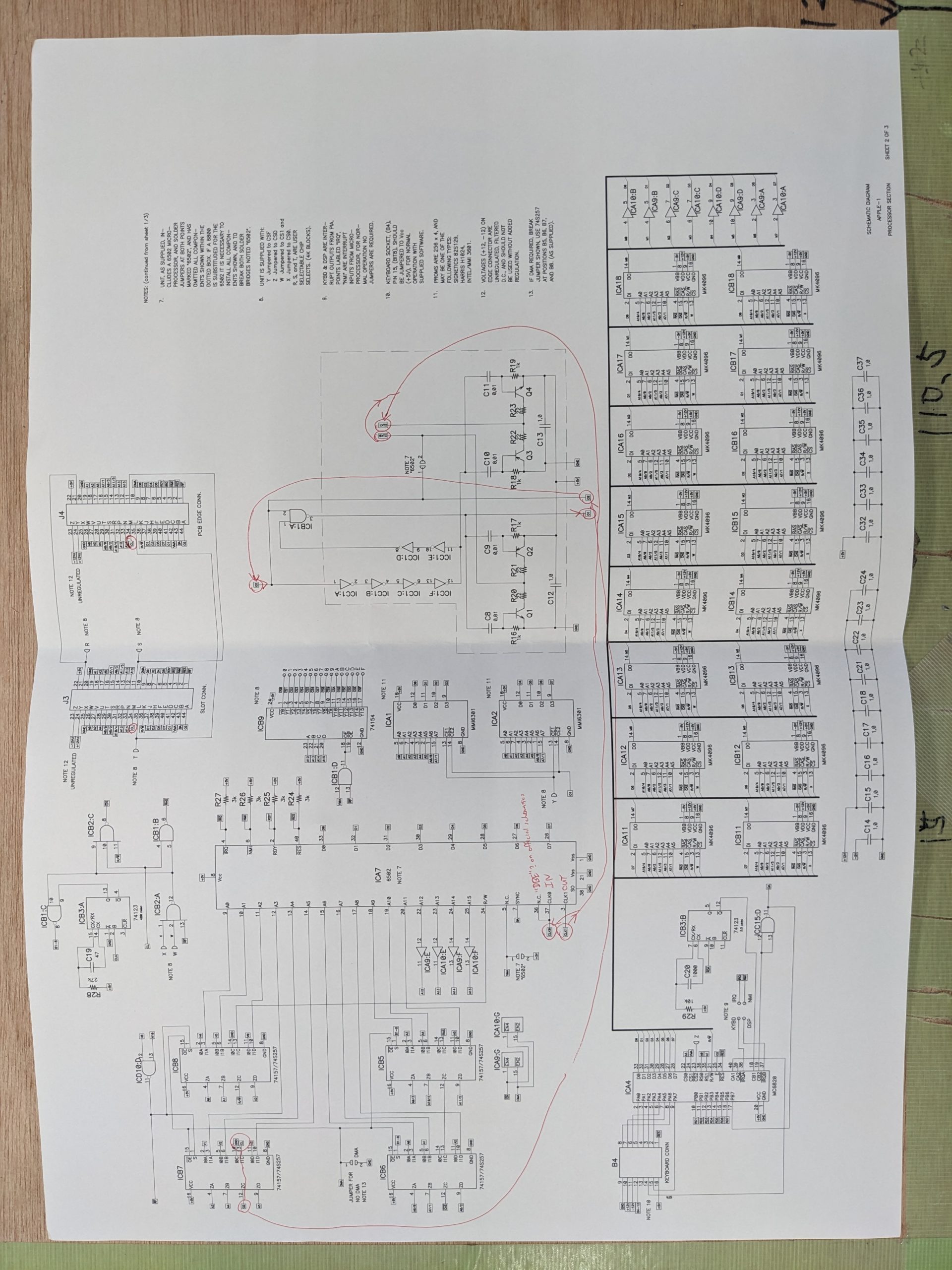
At this point it was time to print out the schematics and study them. Here’s a picture of my annotated Apple 1 schematics that I used to debug the problem:
Teletype section (Note that I cannot guarantee that all my annotations are 100% correct.)CPU section (nothing much annotated here)
Some repair guidelines
There isn’t all that much repair information on the Apple 1, but it’s not too complicated. The computer is basically two devices, a teletype that generates video, and a “computer” section that has the CPU, ROM, and memory. The two devices are linked through an MC6820 chip. There’s one more link; we also get the clock signal for the CPU from teletype section.
One more thing: when you turn on the Apple 1, the CPU isn’t live yet, because there is no reset circuit! (You have to reset the CPU manually using a special key on the keyboard.) So anything that looks too garbage-y right on power up isn’t likely to have much to do with the CPU.
Repair
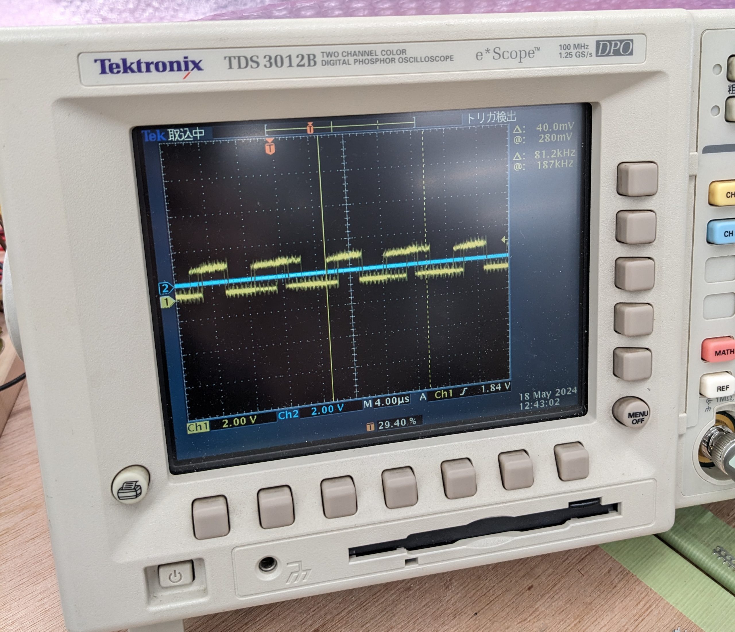
After studying the schematics, I fired up an oscilloscope and traced the oscillator’s output, through the flip-flop, through various counter stages. At this point, a little luck, or a different strategy, would have helped me find the problem rather quickly, but it took at least an hour (probably more) of poking around until I found something obviously out of the ordinary: the “TC” output of the 74160 decade-counter IC was very low. Man, if it had been a Q output I’d have found it in minutes, heh.
74160’s TC output
I removed other chips the TC signal goes to, removed the 74160, checked for shorts to adjacent pins on the board, but couldn’t find anything. Which means the bad signal is produced by the 74160. Perhaps it would work with a slightly higher voltage, so maybe we’ll keep it. So we decided to see if we could get some replacement 74160 ICs (none of that Low-Power Schottky rubbish), and fortunately someone was selling them on Yahoo Auctions! We procured a few and the replacement 74160 made the problem go away!
(74LS160s or even modern HCTs/ACTs/whathaveyous would have likely worked too, but this replica board is proudly populated with original non-LS chips from mostly the 1970s. It’s all fun and games until they say good-bye!)
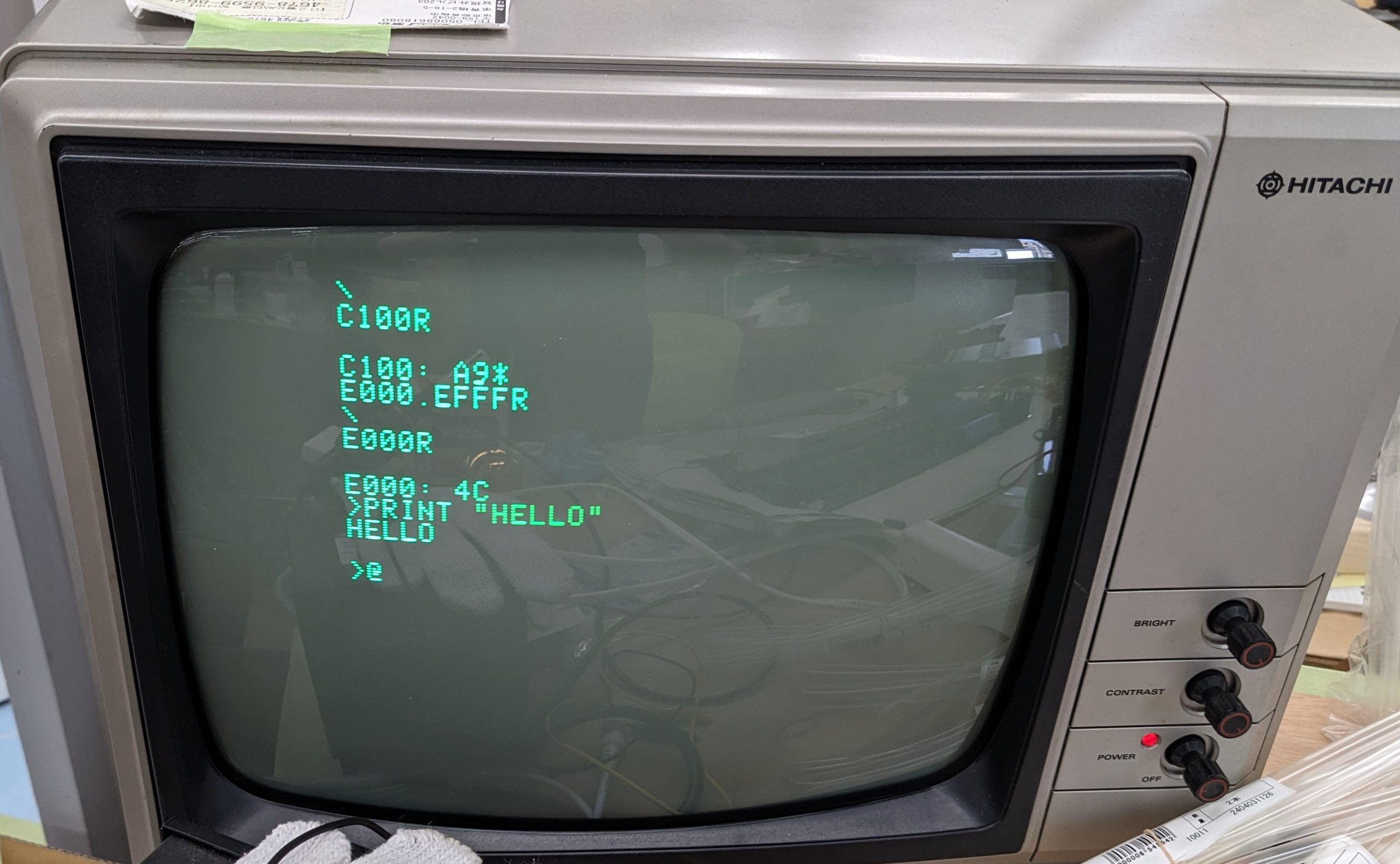
There were no more defects and we were able to boot into Wozmon and load BASIC from tape.
How to boot into BASIC
After powering up, clear the screen and reset the CPU using the dedicated keys. You should get a ‘\’ prompt. Type C100R and enter. This runs the cassette firmware. You should get “C100: A9*”. Then type in E000.EFFFR and at the same time you press enter, start playing the tape. (This loads the BASIC interpreter into memory at 0xE000 to 0xEFFF.) When the audio stops and you get ‘\’ you can start the BASIC interpreter by typing E000R and enter. The BASIC prompt is ‘>’.
The acrylic case
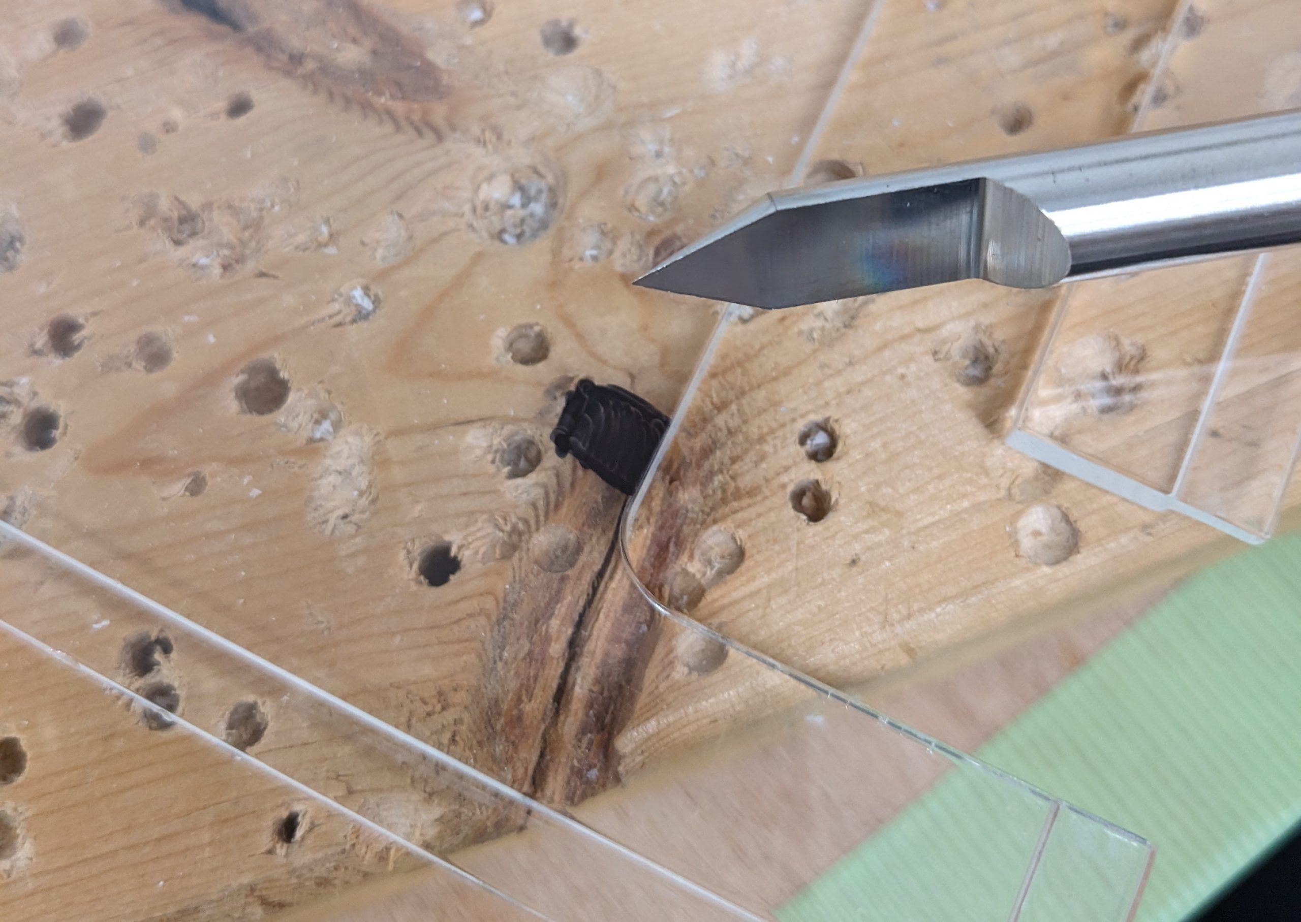
For some reason, the acrylic case that was purchased to put this system into didn’t have the screw holes in the right location, so I had the pleasure of adding more screw holes into the case. (Not just that, the lid needed some trimming in order to fit the cassette board, and we also decided to mod the air inlet/outlet a bit.) And though I didn’t have any experience drilling holes into acrylic (or even a lot of experience drilling anything, really), it actually went really well, using these drill bits specially made for use with acrylic: https://www.amazon.co.jp/dp/B00A630ZRE: Acrysunday アクリル板専用ビット.
It all worked out, mostly. When I did the four holes for the fan I unfortunately didn’t take into account that when screwing the nuts onto the bolts, the nut will obviously add a millimeter (or so) of height vs. just a naked bolt. (The case isn’t that high, so I just had a couple of millimeters I could move the holes up or down.) Putting the nuts on the two top bolts will prevent the lid (the one pictured above) from fitting properly, it would rest on the nuts instead of on the bottom case.
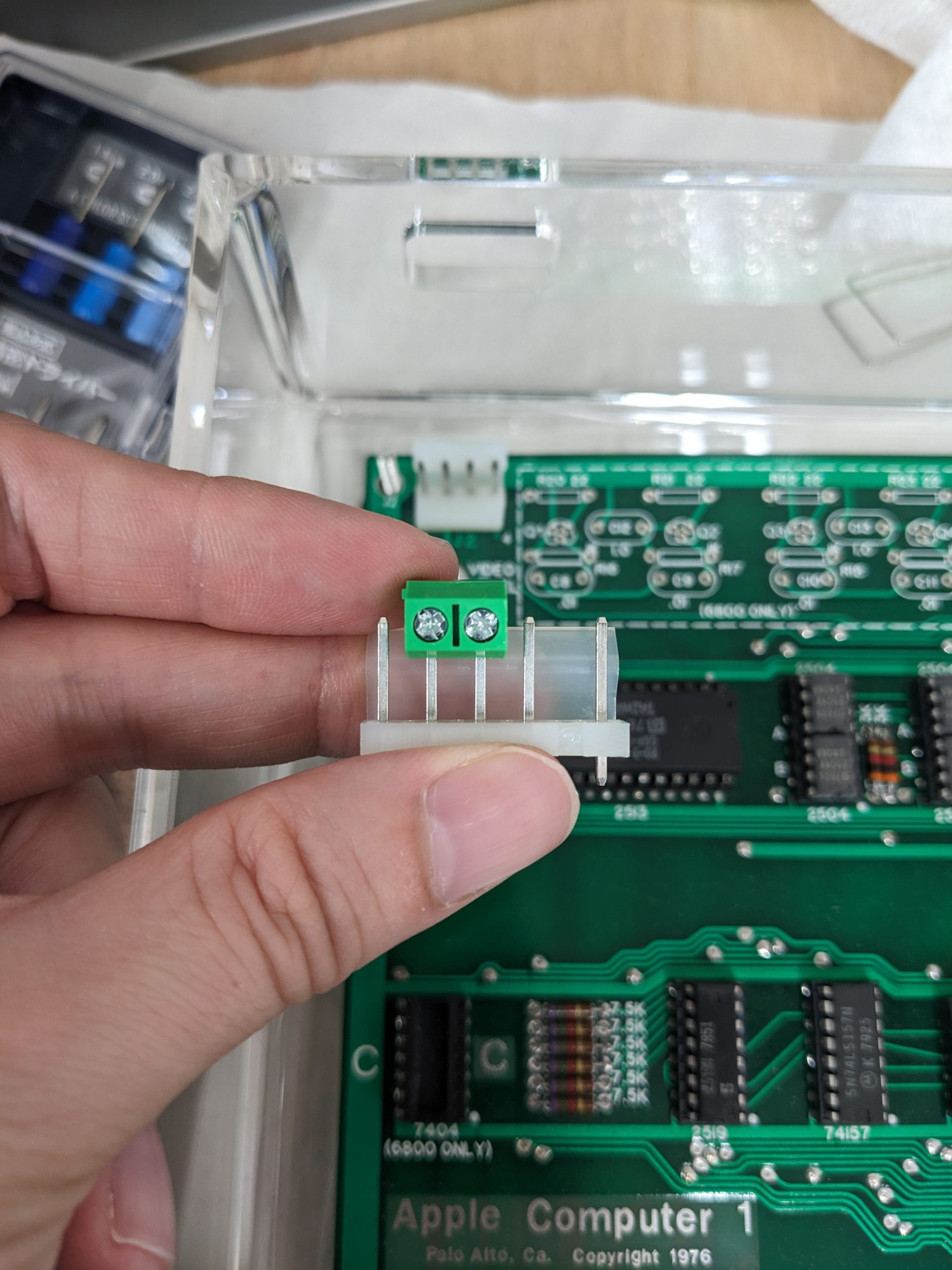
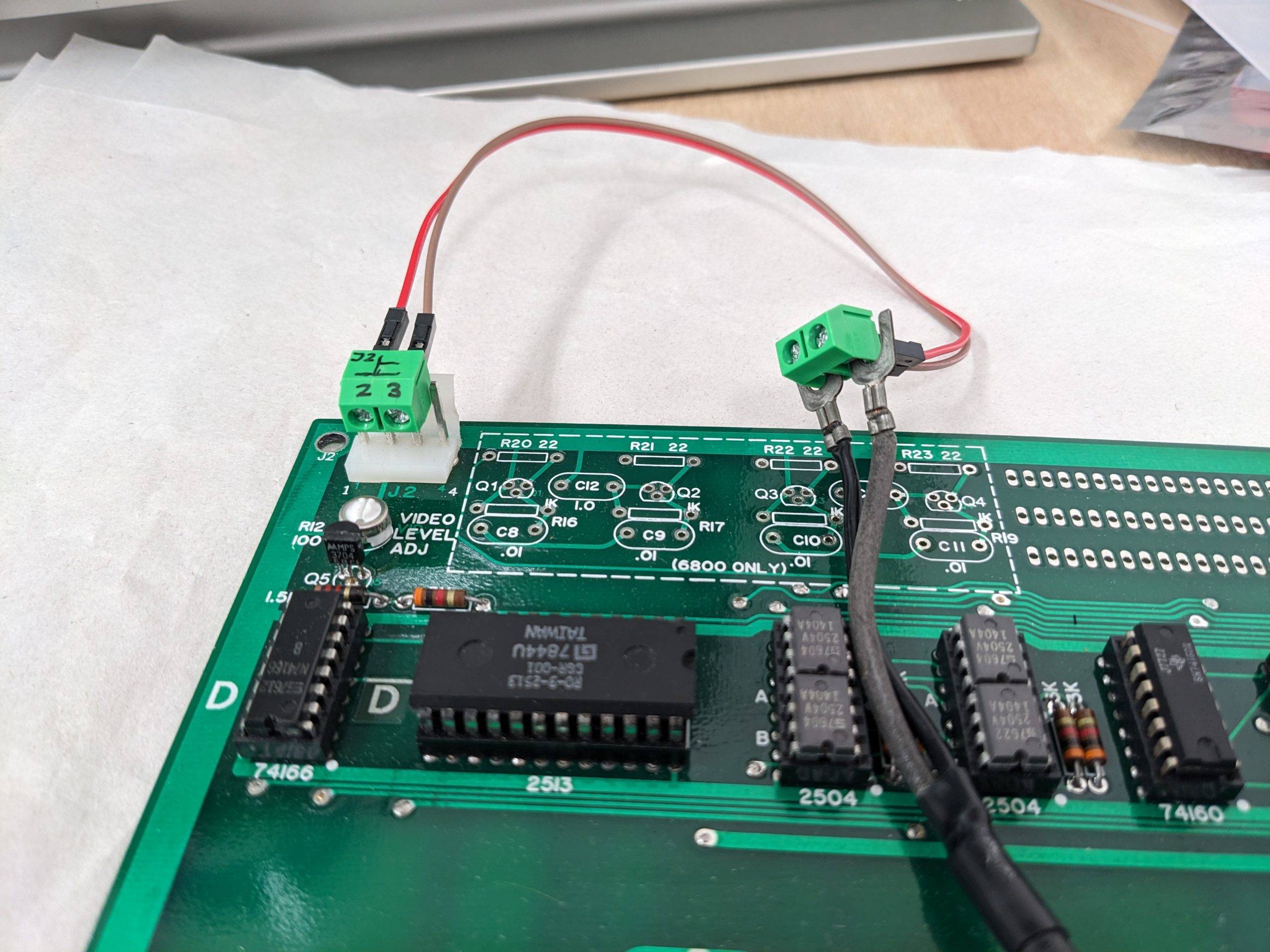
We added some heatsinks on all of the counter ICs, all of which were running rather hot (about 65 degrees after 10 minutes of operation), a powerful fan to blow air on the main voltage regulator (which sucks air through a filter so we don’t end up with a bunch of dust inside), and made a make-shift connector for the video port (J2).
Makeshift video connector using screw terminals: general ideaMakeshift video connector: placed on J2 and connected to TV input


